Publication
Metrics
Quick Actions
AI Quick Summary
This research demonstrates the creation of ultra-thin barrier AlBN/GaN high electron mobility transistors (HEMTs) using a polarization-induced 2D electron gas at an epitaxial AlBN/GaN heterojunction, achieving high current densities and transconductance. However, performance is currently limited by contact resistance.
Quick Answers
What is "Epitaxial high-K AlBN barrier GaN HEMTs" about?
This research demonstrates the creation of ultra-thin barrier AlBN/GaN high electron mobility transistors (HEMTs) using a polarization-induced 2D electron gas at an epitaxial AlBN/GaN heterojunction, achieving high current densities and transconductance. However, performance is currently limited by contact resistance.
What methodology did the authors use?
The research utilizes molecular beam epitaxy (MBE) to grow epitaxial AlBN/GaN heterostructures on 6H-SiC substrates, followed by fabrication of high electron mobility transistors (HEMTs) with ultra-thin AlBN barriers. More in Methodology →
What are the key results?
Realization of polarization-induced 2DEG at the AlBN/GaN heterojunction with current densities exceeding 0.25 A/mm. — Low pinch-off voltage of -0.43 V and peak transconductance of 0.14 S/mm in preliminary HEMT realization. More in Key Results →
Why is this work significant?
This work offers a promising alternative to current GaN transistors by extending their performance using epitaxial high-K AlBN barrier layers, which can provide both polarization-induced 2DEG and appropriate insulating properties for GaN HEMTs in power electronics and RF/mm-wave applications. More in Significance →
What are the main limitations?
Current transistor performance is limited by contact resistance. — The study does not explore long-term device reliability or operational stability under various environmental conditions. More in Limitations →
Abstract
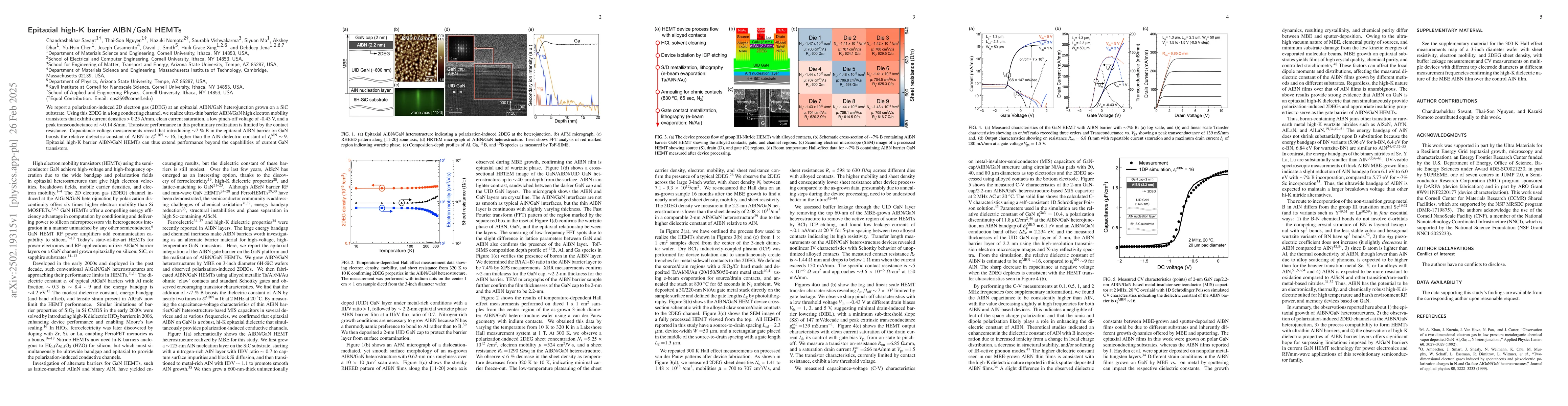
We report a polarization-induced 2D electron gas (2DEG) at an epitaxial AlBN/GaN heterojunction grown on a SiC substrate. Using this 2DEG in a long conducting channel, we realize ultra-thin barrier AlBN/GaN high electron mobility transistors that exhibit current densities of more than 0.25 A/mm, clean current saturation, a low pinch-off voltage of -0.43 V, and a peak transconductance of 0.14 S/mm. Transistor performance in this preliminary realization is limited by the contact resistance. Capacitance-voltage measurements reveal that introducing 7 % B in the epitaxial AlBN barrier on GaN boosts the relative dielectric constant of AlBN to 16, higher than the AlN dielectric constant of 9. Epitaxial high-K barrier AlBN/GaN HEMTs can thus extend performance beyond the capabilities of current GaN transistors.
AI Key Findings
Generated Jun 11, 2025
Methodology — What approach did the authors take?
The research utilizes molecular beam epitaxy (MBE) to grow epitaxial AlBN/GaN heterostructures on 6H-SiC substrates, followed by fabrication of high electron mobility transistors (HEMTs) with ultra-thin AlBN barriers.
Key Results — What are the main findings?
- Realization of polarization-induced 2DEG at the AlBN/GaN heterojunction with current densities exceeding 0.25 A/mm.
- Low pinch-off voltage of -0.43 V and peak transconductance of 0.14 S/mm in preliminary HEMT realization.
- Capacitance-voltage measurements show that 7% B in the epitaxial AlBN barrier boosts its relative dielectric constant to 16, higher than AlN's 9.
- Demonstrated large-area growth of AlBN/GaN heterostructures across a 3-inch wafer with consistent 2DEG properties.
- Higher capacitance observed for AlBN barrier-based MIS capacitors compared to control AlN barrier-based devices with comparable top electrode sizes and barrier thicknesses.
Significance — Why does this research matter?
This work offers a promising alternative to current GaN transistors by extending their performance using epitaxial high-K AlBN barrier layers, which can provide both polarization-induced 2DEG and appropriate insulating properties for GaN HEMTs in power electronics and RF/mm-wave applications.
Technical Contribution — What is the technical contribution?
The research presents a novel approach to utilizing boron-containing AlBN as an epitaxial high-K dielectric layer in GaN HEMTs, demonstrating its potential to surpass limitations posed by conventional AlGaN barriers.
Novelty — What is new about this work?
This study distinguishes itself by employing MBE-grown AlBN thin films with enhanced dielectric constants, showcasing their compatibility with GaN-based HEMTs for improved performance in power electronics and RF devices.
Limitations — What are the limitations of this study?
- Current transistor performance is limited by contact resistance.
- The study does not explore long-term device reliability or operational stability under various environmental conditions.
- Further optimization of growth conditions and device processing is needed to fully harness the potential of AlBN barriers.
Future Work — What did the authors propose for future work?
- Investigate methods to reduce contact resistance for improved transistor performance.
- Conduct reliability and stability tests under different operating conditions.
- Explore the integration of AlBN barriers in more complex device architectures for advanced applications.
Paper Details
How to Cite This Paper
@article{dhar2025epitaxial,
title = {Epitaxial high-K AlBN barrier GaN HEMTs},
author = {Dhar, Akshey and Savant, Chandrashekhar and Smith, David J. and others},
year = {2025},
eprint = {2502.19315},
archivePrefix = {arXiv},
primaryClass = {physics.app-ph},
}
Dhar, A., Savant, C., Smith, D., Jena, D., Xing, H., Casamento, J., Nomoto, K., Vishwakarma, S., Ma, S., Nguyen, T., & Chen, Y. (2025). Epitaxial high-K AlBN barrier GaN HEMTs. arXiv. https://arxiv.org/abs/2502.19315
Dhar, Akshey, et al. "Epitaxial high-K AlBN barrier GaN HEMTs." arXiv, 2025, arxiv.org/abs/2502.19315.
PDF Preview
Citation Network
Current paper (gray), citations (green), references (blue)
Display is limited for performance on very large graphs.
Similar Papers
Found 4 papersCharacterization of GaN-based HEMTs Down to 4.2 K for Cryogenic Applications
Haochen Zhang, Yuanke Zhang, Yue Sun et al.
No citations found for this paper.
Comments (0)