Academic Profile
Statistics
Similar Authors
Papers on arXiv
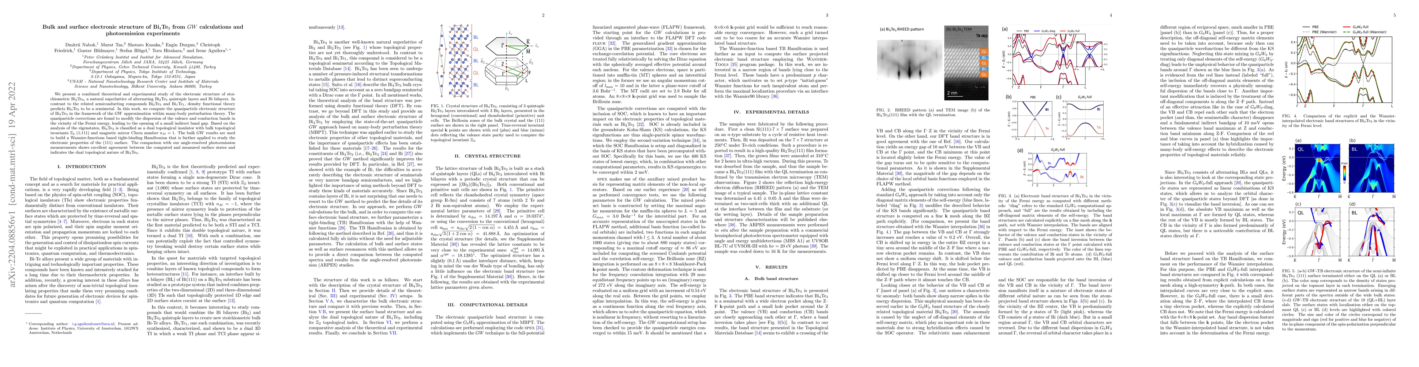
We present a combined theoretical and experimental study of the electronic structure of stoichiometric Bi$_4$Te$_3$, a natural superlattice of alternating Bi$_2$Te$_3$ quintuple layers and Bi bilaye...
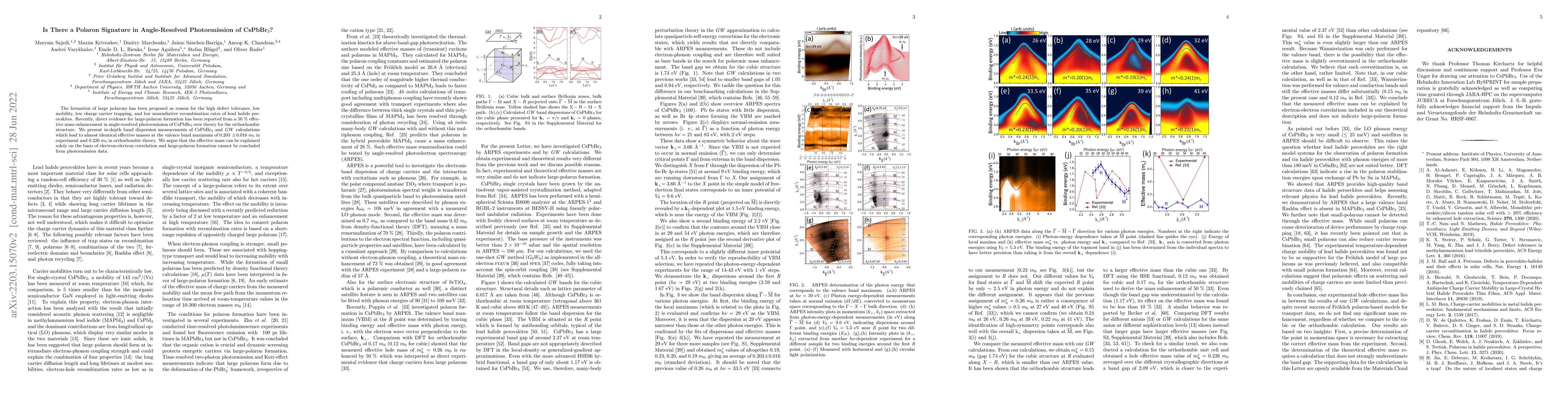
The formation of large polarons has been proposed as reason for the high defect tolerance, low mobility, low charge carrier trapping and low nonradiative recombination rates of lead halide perovskit...
Most traditional semiconductor materials are based on the control of doping densities to create junctions and thereby functional and efficient electronic and optoelectronic devices. The technology d...
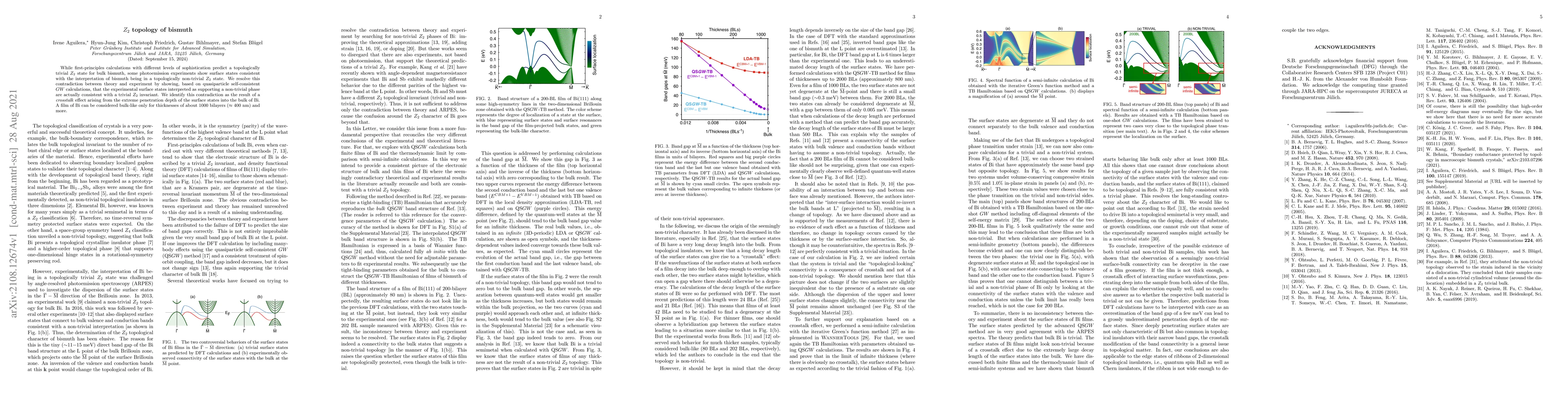
While first-principles calculations with different levels of sophistication predict a topologically trivial $Z_2$ state for bulk bismuth, some photoemission experiments show surface states consisten...
In this work, we studied the bulk band structure of a topological insulator (TI) Bi2Se3 and determined the contributions of the Bi and Se orbital states to the valence bands using standing wave-exci...
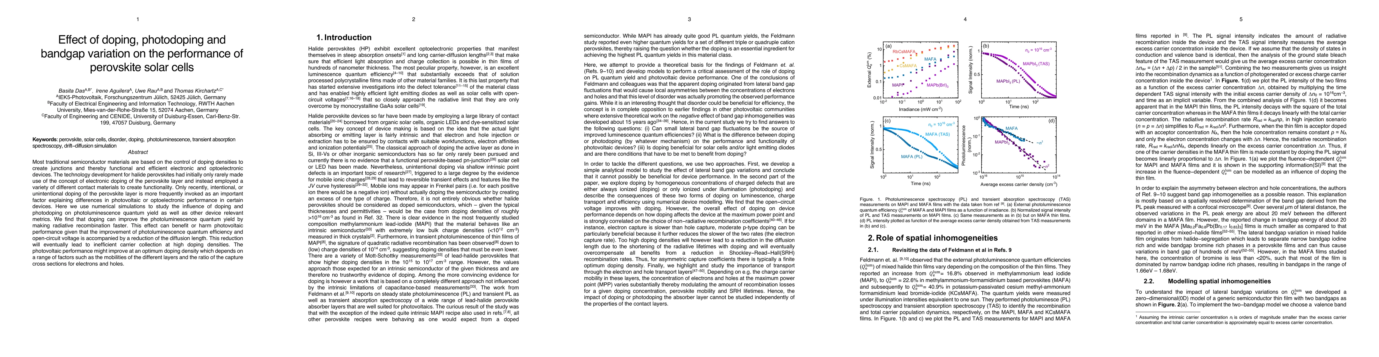
The term defect tolerance is widely used in literature to describe materials such as lead-halides which exhibit long non-radiative lifetimes of carriers despite possessing a large concentration of p...
We develop a numerical scheme for the calculation of tunneling current $I$ and differential conductance $\mathsf{d}I/\mathsf{d}V$ of metal and CO-terminated STM tips on the topological insulators $\ma...
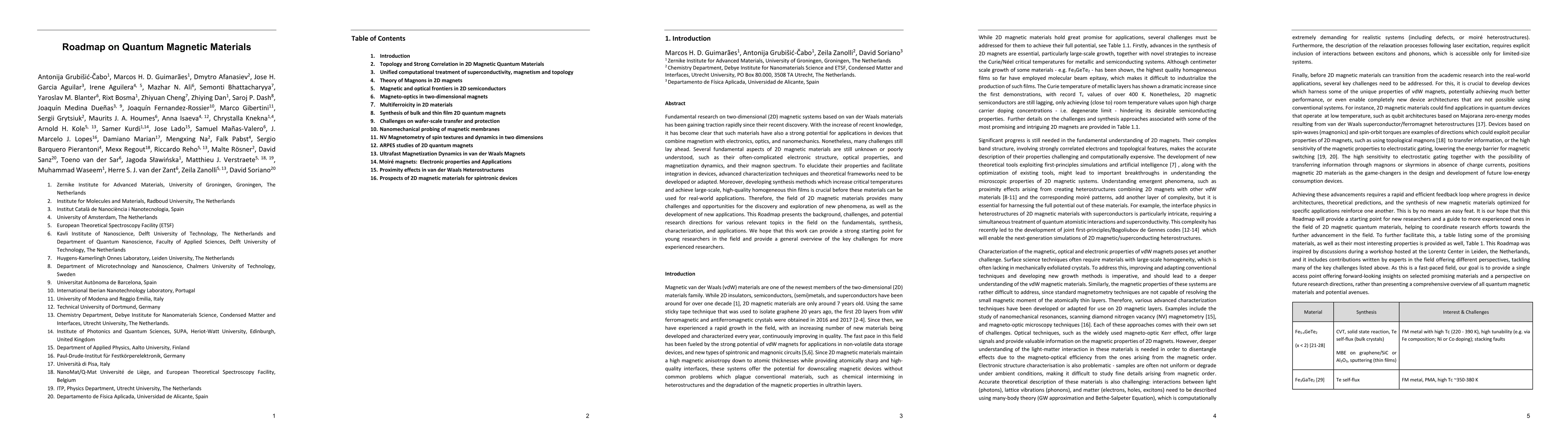
Fundamental research on two-dimensional (2D) magnetic systems based on van der Waals materials has been gaining traction rapidly since their recent discovery. With the increase of recent knowledge, it...