Publication
Metrics
Paper Preview
Abstract
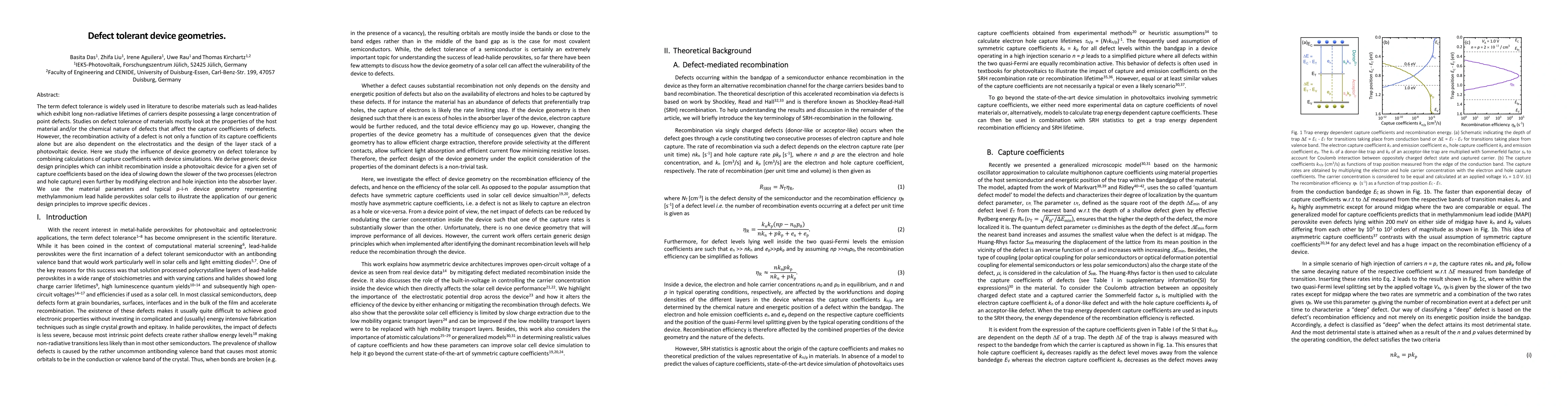
The term defect tolerance is widely used in literature to describe materials such as lead-halides which exhibit long non-radiative lifetimes of carriers despite possessing a large concentration of point defects. Studies on defect tolerance of materials mostly look at the properties of the host material and/or the chemical nature of defects that affect the capture coefficients of defects. However, the recombination activity of a defect is not only a function of its capture coefficients alone but are also dependent on the electrostatics and the design of the layer stack of a photovoltaic device. Here we study the influence of device geometry on defect tolerance by combining calculations of capture coefficients with device simulations. We derive generic device design principles which can inhibit recombination inside a photovoltaic device for a given set of capture coefficients based on the idea of slowing down the slower of the two processes (electron and hole capture) even further by modifying electron and hole injection into the absorber layer. We use the material parameters and typical p-i-n device geometry representing methylammonium lead halide perovskites solar cells to illustrate the application of our generic design principles to improve specific devices .
AI Key Findings
Get AI-generated insights about this paper's methodology, results, significance, and more — seven facets brought into focus.
Impact
Paper Details
Authors
PDF Preview
Key Terms
Citation Network
Current paper (gray), citations (green), references (blue)
Display is limited for performance on very large graphs.
Discussion 0