Academic Profile
Statistics
Similar Authors
Papers on arXiv
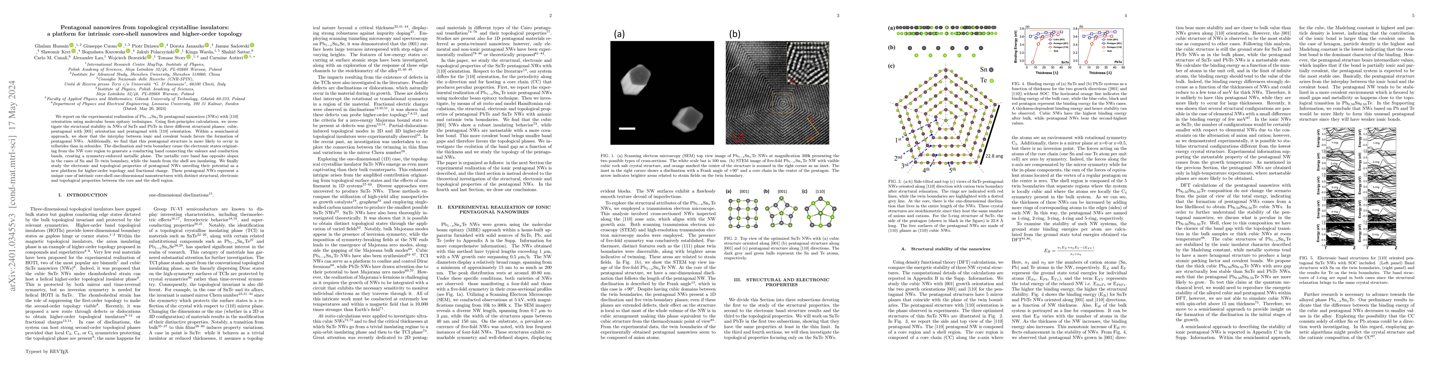
We report on the experimental realization of Pb1-xSnxTe pentagonal nanowires (NWs) with [110] orientation using molecular beam epitaxy techniques. Using first-principles calculations, we investigate...
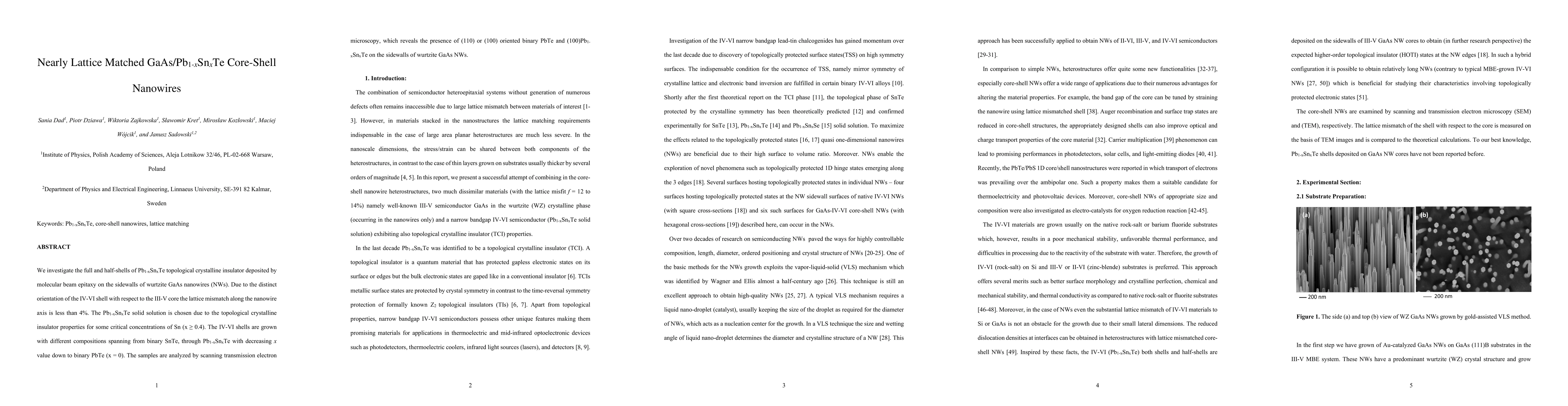
We investigate the full and half-shells of Pb(1-x)Sn(x)Te topological crystalline insulator deposited by molecular beam epitaxy on the sidewalls of wurtzite GaAs nanowires (NWs). Due to the distinct...
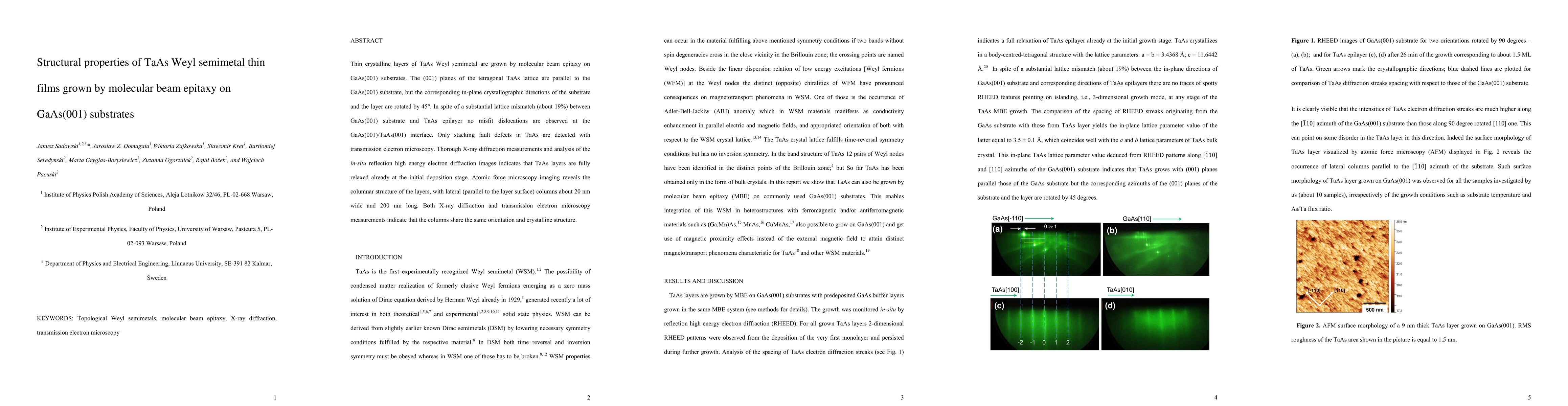
Thin crystalline layers of TaAs Weyl semimetal (9 and 18 nm thick) are grown by molecular beam epitaxy on GaAs(001) substrates. The (001) planes of the tetragonal TaAs lattice are parallel to the Ga...
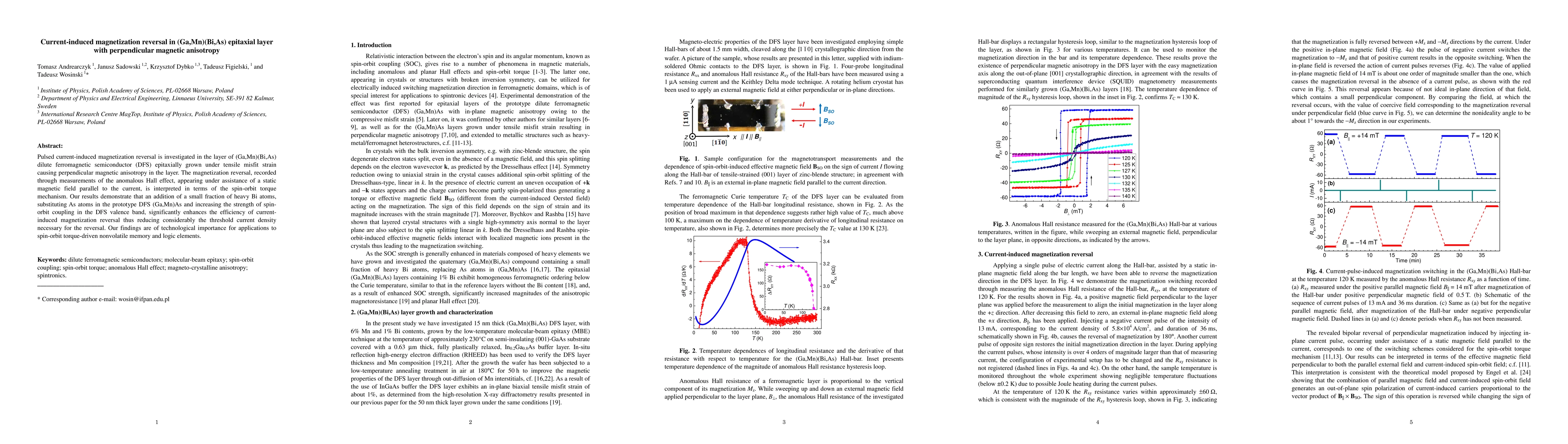
Pulsed current-induced magnetization reversal is investigated in the layer of (Ga,Mn)(Bi,As) dilute ferromagnetic semiconductor (DFS) epitaxially grown under tensile misfit strain causing perpendicu...
Incorporation of Bi into GaAs-(Ga,Al)As-Ga(As,Bi) core-shell nanowires grown by molecular beam epitaxy is studied with transmission electron microscopy. Nanowires are grown on GaAs(111)B substrates ...
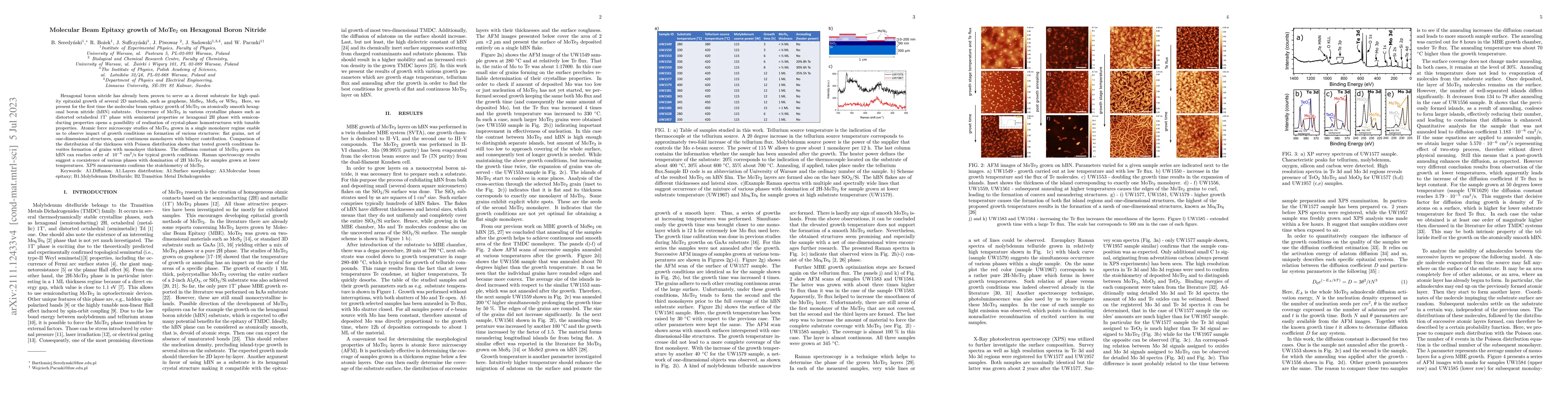
Hexagonal boron nitride has already been proven to serve as a decent substrate for high quality epitaxial growth of several 2D materials, such as graphene, MoSe$_{\tiny{\textrm{2}}}$, MoS$_{\tiny{\t...
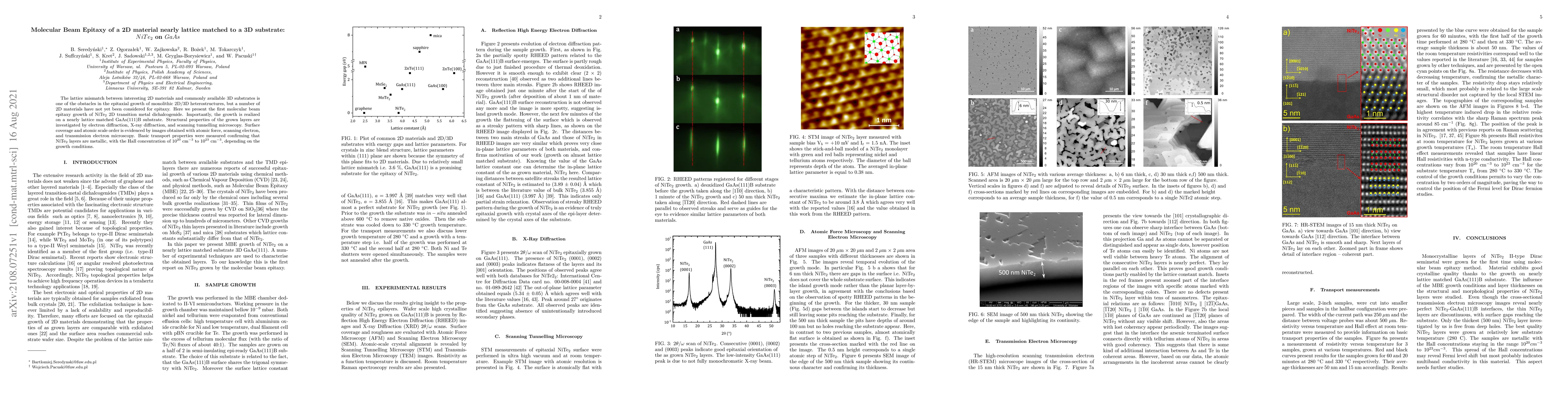
The lattice mismatch between interesting 2D materials and commonly available 3D substrates is one of the obstacles in the epitaxial growth of monolithic 2D/3D heterostructures, but a number of 2D ma...
Here we report on detailed studies of the magnetic properties of the wurtzite (Ga,Mn)As cylindrical shells. Ga$_{0.94}$Mn$_{0.06}$As shells have been grown by molecular beam epitaxy at low temperatu...
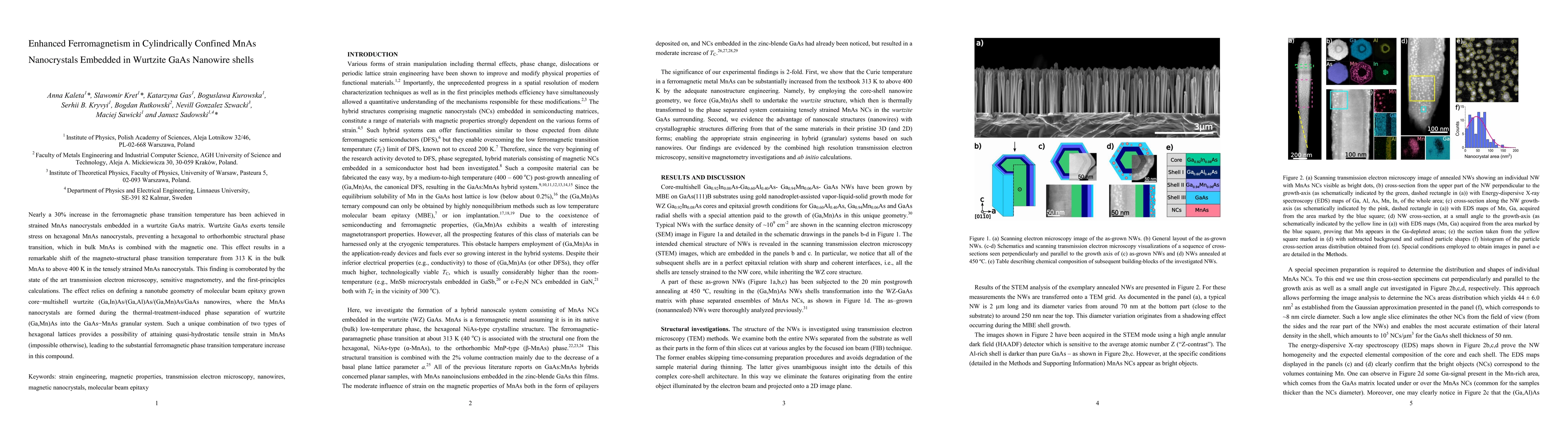
Nearly 30% increase of the ferromagnetic phase transition temperature has been achieved in strained MnAs nanocrystals embedded in a wurtzite GaAs matrix. Wurtzite GaAs exerts tensile stress on hexag...
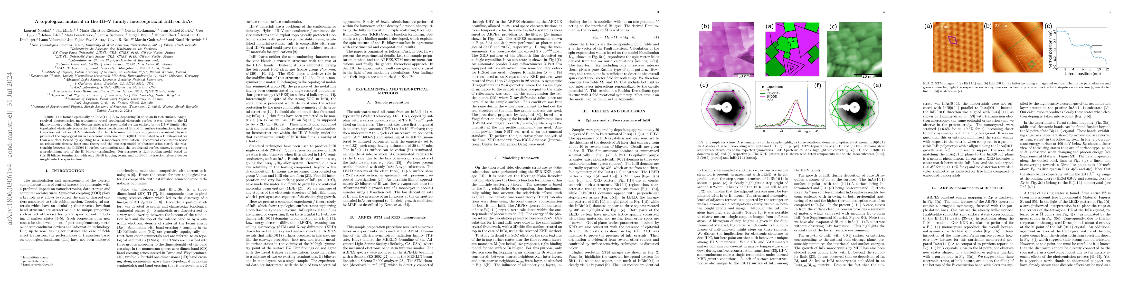
InBi(001) is formed epitaxially on InAs(111)-A by depositing Bi on to an In-rich surface. Angle-resolved photoemission measurements reveal topological electronic surface states, close to the M bar h...

We investigate core/shell GaAs/(Pb,Sn)Te nanowire nanoheterostructures with wurtzite (wz) GaAs cores and (Pb,Sn)Te topological crystalline insulator shells. The nanostructures have been grown by molec...