This paper investigates the structural properties of TaAs Weyl semimetal thin films grown on GaAs(001) substrates via molecular beam epitaxy, revealing a fully relaxed epilayer with no misfit dislocations despite a 19% lattice mismatch, and a columnar structure with uniform orientation and crystalline arrangement.
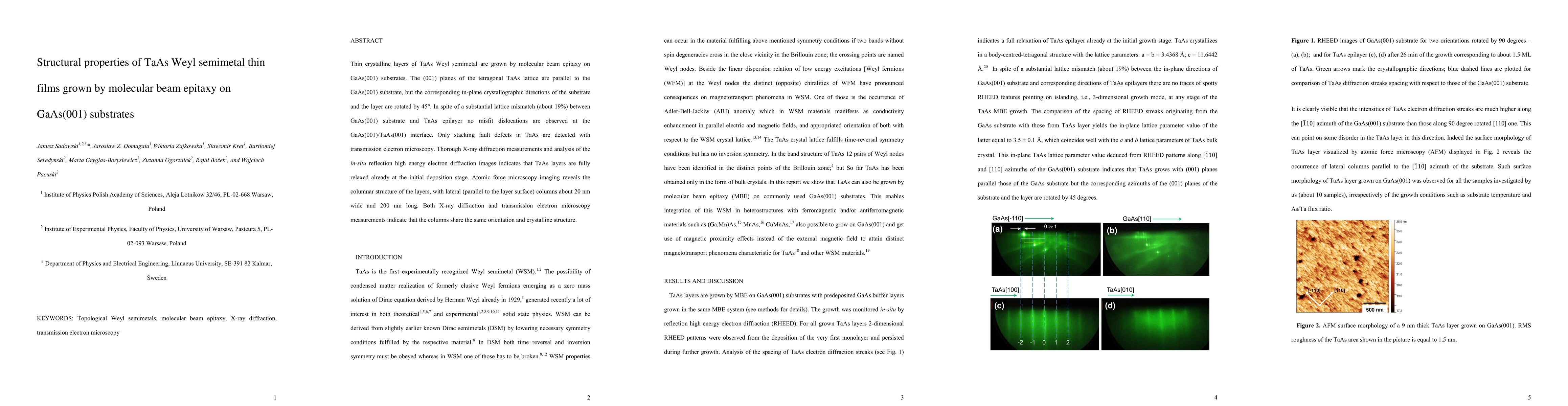
Thin crystalline layers of TaAs Weyl semimetal (9 and 18 nm thick) are grown by molecular beam epitaxy on GaAs(001) substrates. The (001) planes of the tetragonal TaAs lattice are parallel to the GaAs(001) substrate, but the corresponding in-plane crystallographic directions of the substrate and the layer are rotated by 45{\deg}. In spite of a substantial lattice mismatch (about 19%) between GaAs(001) substrate and TaAs epilayer no misfit dislocations are observed at the GaAs(001)/TaAs(001) interface. Only stacking fault defects in TaAs are detected with transmission electron microscopy. Thorough X-ray diffraction measurements and analysis of the in-situ reflection high energy electron diffraction images indicates that TaAs layers are fully relaxed already at the initial deposition stage. Atomic force microscopy imaging reveals the columnar structure of the layers, with lateral (parallel to the layer surface) columns about 20 nm wide and 200 nm long. Both X-ray diffraction and transmission electron microscopy measurements indicate that the columns share the same orientation and crystalline structure.
This graph shows how this paper is connected to other research. The current paper is shown in dark gray, papers that cite it are in green, and papers it references are in blue. You can:
• Hover over any node to see the paper title
• Click a node to view that paper's details
• Drag nodes to rearrange the graph
• Use the zoom controls (bottom right) to zoom in/out
Title | Authors | Year | Actions |
---|---|---|---|
Tutorial: Defects in topological semimetals
|
Kirstin Alberi, Chase Brooks, Ian A. Leahy, Stephan Lany
|
2024
|
View Paper |
Anisotropic weak antilocalization in thin films of the Weyl semimetal TaAs
|
Ian A. Leahy, A. Rice, Chun-Sheng Jiang, Goutam Paul, Kirstin Alberi, J. Nelson
|
2024
|
View Paper |
Heteroepitaxial Growth of InBi(001)
|
T. J. Rehaag, G. R. Bell
|
2024
|
View Paper |
Ultra-broadband and wide-angle nonreciprocal thermal emitter based on Weyl semimetal metamaterials
|
K. Shi, Yuwei Sun, Run Hu, Sailing He
|
2024
|
View Paper |
Large area crystalline Weyl semimetal with nano Au film based micro-fold line array for THz detector
|
Qinghao Song, Yu Zhou, ErSe Jia, Jiatong Wang, M. Zhang, Bingyuan Zhang
|
2023
|
View Paper |
Uniting Weyl semimetals and semiconductors in a family of arsenides
|
W. Pacuski
|
2023
|
View Paper |
Broadband and Wide Angle Nonreciprocal Thermal Emission from Weyl Semimetal Structures
|
A. Butler, C. Argyropoulos
|
2023
|
View Paper |
Thin film growth of the Weyl semimetal NbAs
|
W. Yanez, Yu-Sheng Huang, Supriya Ghosh, Saurav Islam, Emma Steinebronn, A. Richardella, K. Mkhoyan, N. Samarth
|
2023
|
View Paper |
Epitaxial Integration of Dirac Semimetals with Si(001)
|
A. Rice, K. Alberi
|
2023
|
View Paper |
Thin-film TaAs: Developing a platform for Weyl semimetal devices
|
J. Nelson, A. Rice, R. Kurleto, Amanda Shackelford, Zachary Sierzega, Peipei Hao, Bryan S Berggren, Chun-Sheng Jiang, A. Norman, M. Holtz, J. Mangum, I. Leahy, K. Heinselman, H. Ness, Mark van Schilfgaarde, D. Dessau, K. Alberi
|
2023
|
View Paper |
Published: 2009-11-10
Comments (0)