Academic Profile
Statistics
Similar Authors
Papers on arXiv
The exotic topological domains in ferroelectrics and multiferroics have attracted extensive interest in recent years due to their novel functionalities and potential applications in nanoelectronic d...
The coupling of mechanical deformation and electrical stimuli at the nanoscale has been a subject of intense investigation in the realm of materials science. Recently, twisted van der Waals (vdW) ma...
Particle-like topologies, such as vortex-antivortex (V-AV) pairs, have garnered significant attention in the field of condensed matter. However, the detailed phase transition dynamics of V-AV pairs,...
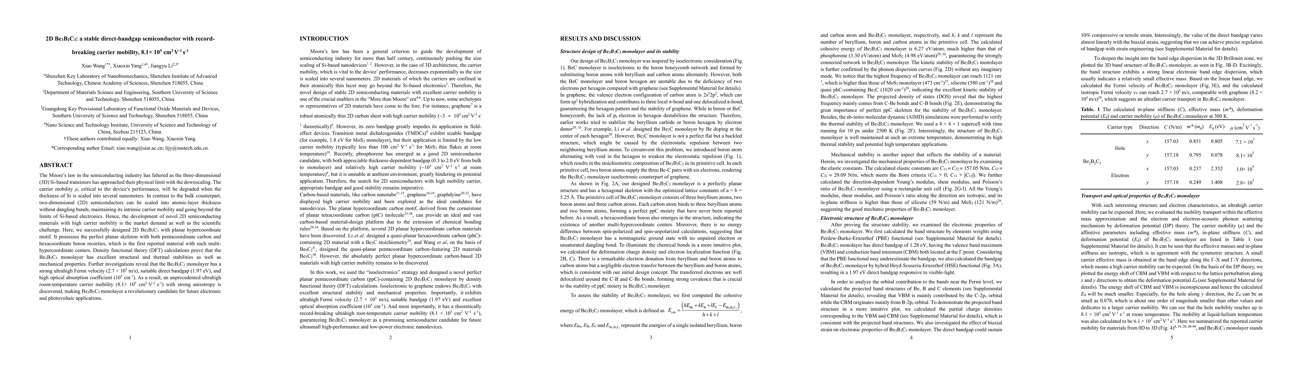
The Moore's law in the semiconducting industry has faltered as the three-dimensional (3D) Si-based transistors has approached their physical limit with the downscaling. The carrier mobility $\rm \mu...
A double moir\'e superlattice can be realized by stacking three layers of atomically thin two-dimensional materials with designer interlayer twisting or lattice mismatches. In this novel structure, ...
Defects in organic-inorganic hybrid perovskites (OIHPs) greatly influence their optoelectronic properties. Identification and better understanding of defects existing in OIHPs is an essential step t...
Room-temperature polar skyrmion bubbles that are recently found in oxide superlattice, have received enormous interests for their potential applications in nanoelectronics due to the nanometer size,...
Understanding the atomic structure and structural instability of organic-inorganic hybrid perovskites is the key to appreciate their remarkable photoelectric properties and failure mechanism. Here, ...
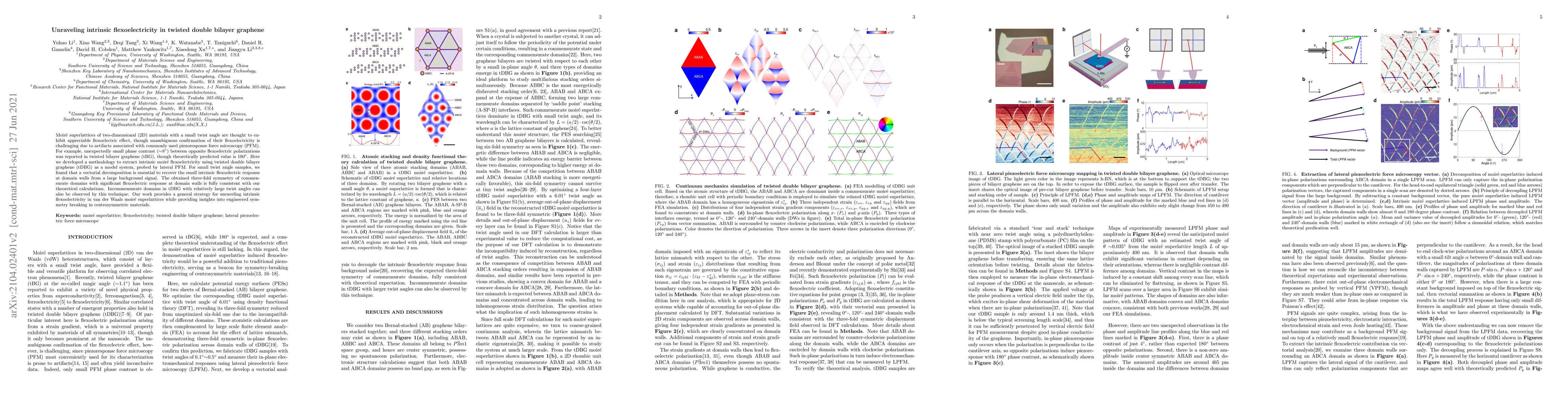
Moir\'e superlattices of two-dimensional (2D) materials with a small twist angle are thought to exhibit appreciable flexoelectric effect, though unambiguous confirmation of their flexoelectricity is...
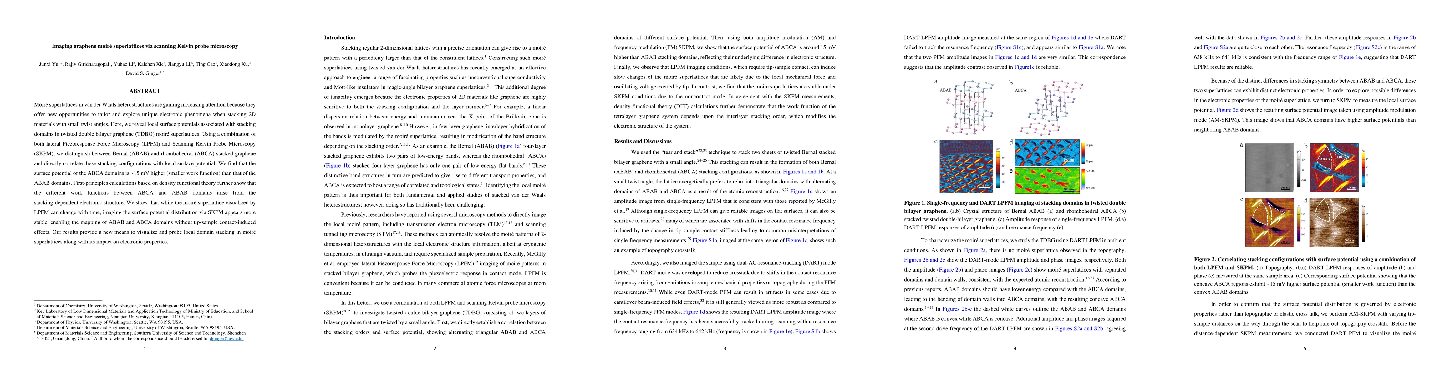
Moir\'e superlattices in van der Waals heterostructures are gaining increasing attention because they offer new opportunities to tailor and explore unique electronic phenomena when stacking 2D mater...
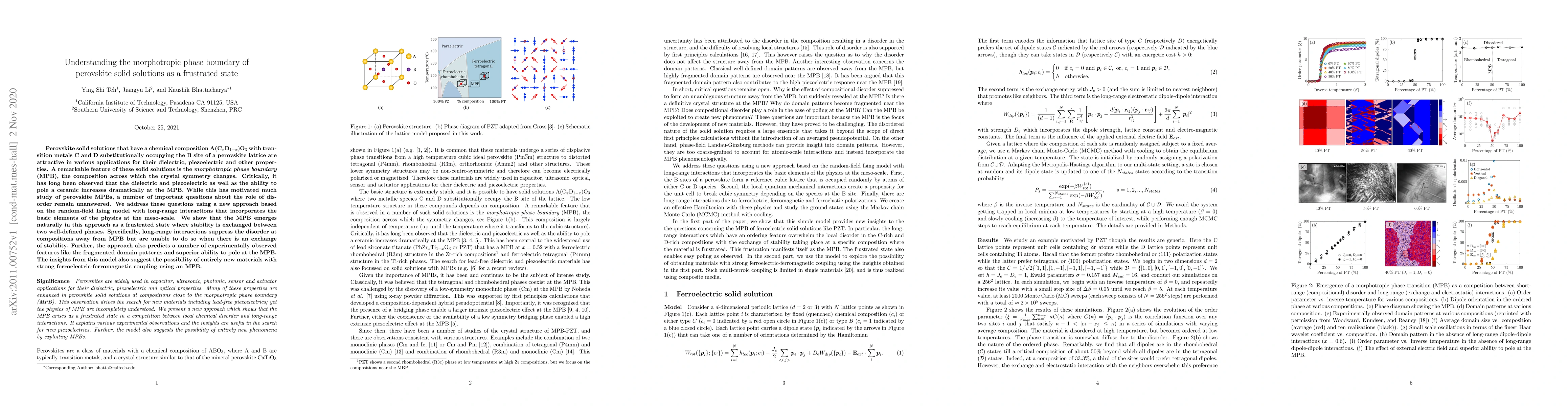
Perovskite solid solutions that have a chemical composition A(C$_x$D$_{1-x})$O$_3$ with transition metals C and D substitutionally occupying the B site of a perovskite lattice are attractive in vari...
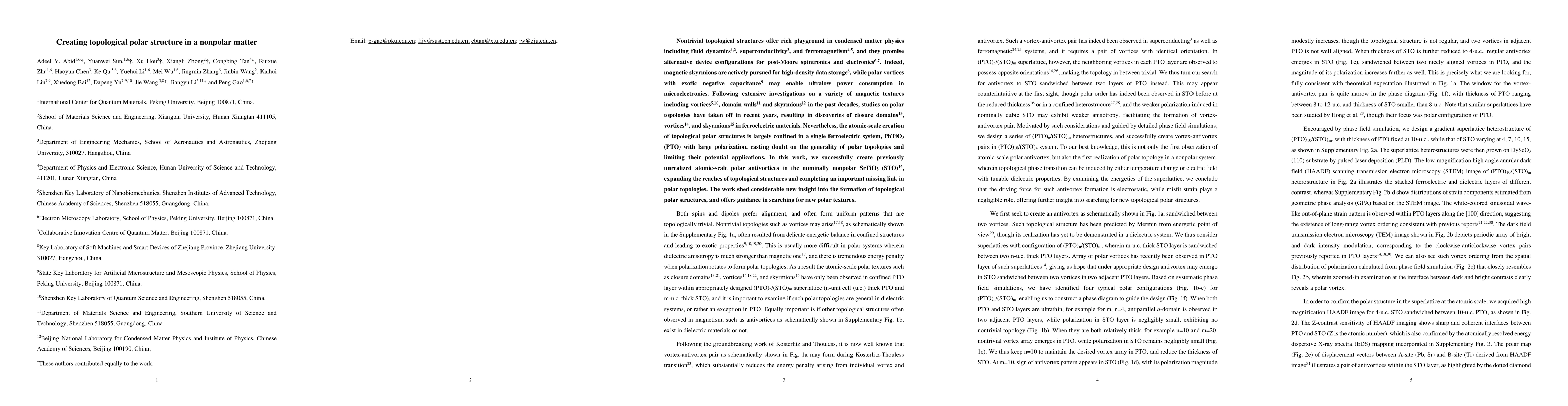
Nontrivial topological structures offer rich playground in condensed matter physics including fluid dynamics, superconductivity, and ferromagnetism, and they promise alternative device configuration...
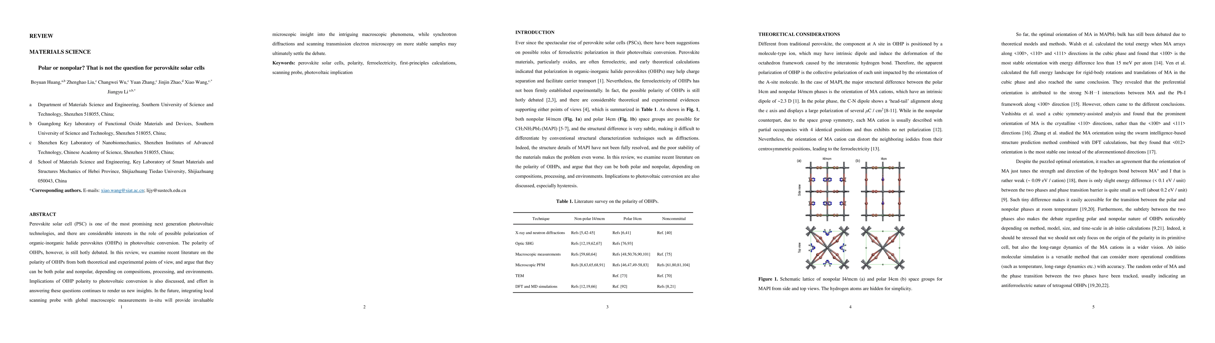
Perovskite solar cell (PSC) is one of the most promising next generation photovoltaic technologies, and there are considerable interests in the role of possible polarization of organic-inorganic hal...
Organic-inorganic hybrid perovskites (OIHPs) have attracted extensive research interest as a promising candidate for efficient and inexpensive solar cells. Transmission electron microscopy character...
Ever increasing hardware capabilities and computation powers have made acquisition and analysis of big scientific data at the nanoscale routine, though much of the data acquired often turns out to b...
Artificial intelligence (AI) and machine learning have promised to revolutionize the way we live and work, and one of particularly promising areas for AI is image analysis. Nevertheless, many curren...
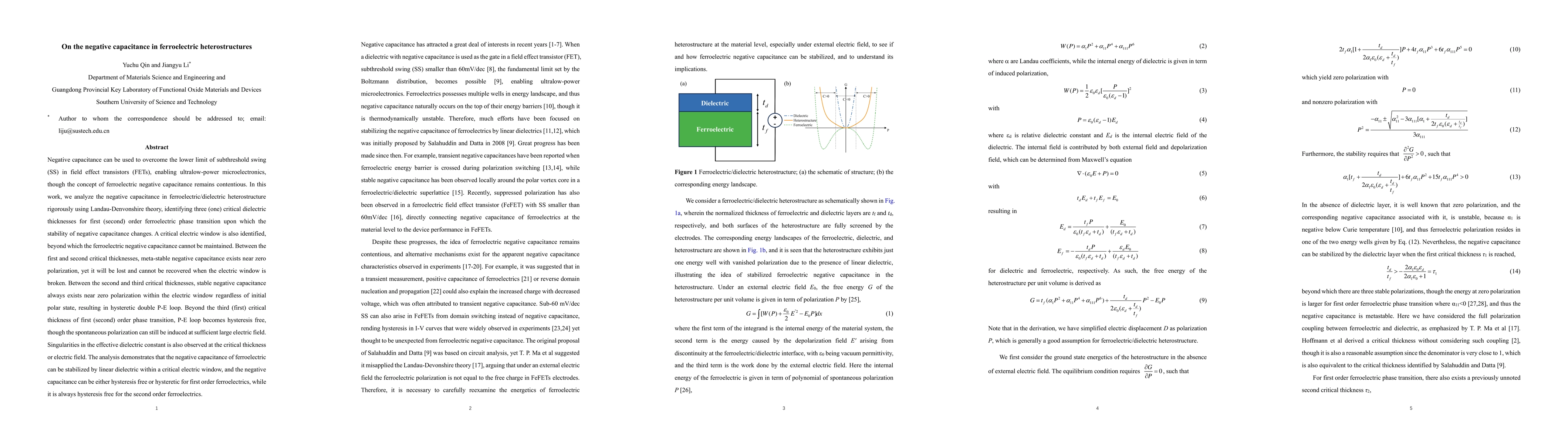
Negative capacitance can be used to overcome the lower limit of subthreshold swing (SS) in field effect transistors (FETs), enabling ultralow-power microelectronics, though the concept of ferroelectri...

Piezoelectric and ferroelectric wurtzite are promising to reshape modern microelectronics because they can be easily integrated with mainstream semiconductor technology. Sc doped AlN (Al$_{1-x}$Sc$_x$...
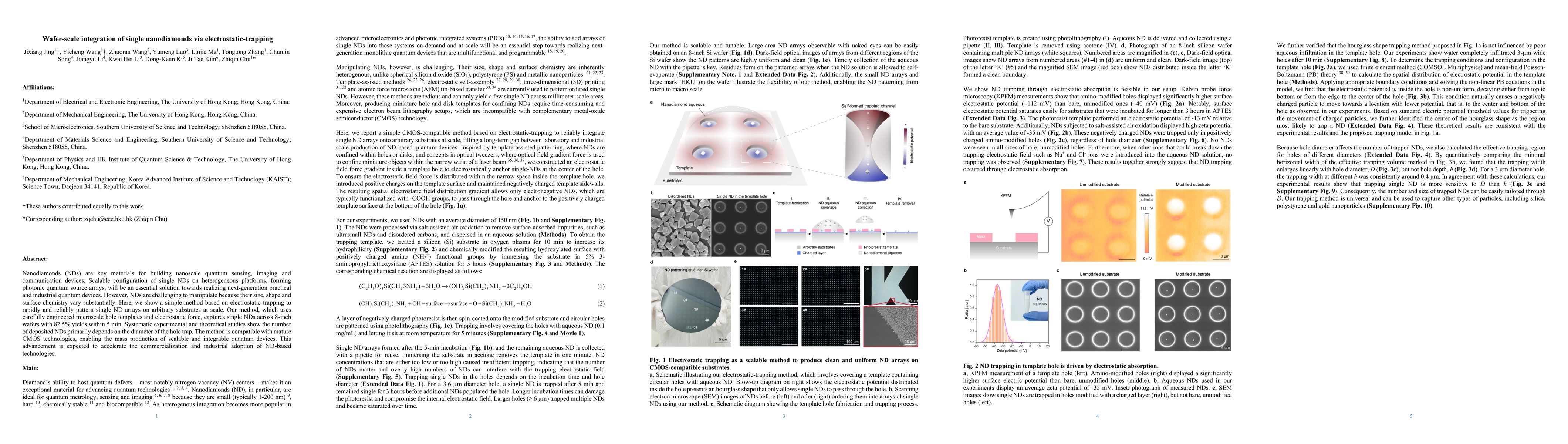
Nanodiamonds (NDs) are key materials for building nanoscale quantum sensing, imaging and communication devices. Scalable configuration of single NDs on heterogeneous platforms, forming photonic quantu...