Publication

Published: Sep 27, 2025
Categories: physics.optics

Metrics

Source: ArXiv

Quick Actions

View PDF

Quick Answers

What methodology did the authors use?

The research employs electrostatic-trapping using microscale hole templates to pattern single nanodiamonds (NDs) on substrates. The method involves photolithography, electrostatic force, and controlled deposition of NDs through template holes. More in Methodology →

What are the key results?

Achieved 82.5% yield of single ND arrays on 8-inch wafers within 5 minutes. — Trapping efficiency is primarily determined by the diameter of the hole template, with smaller holes leading to fewer deposited NDs and larger holes allowing more deposition. More in Key Results →

Why is this work significant?

This advancement enables mass production of quantum devices using nanodiamonds, accelerating commercialization of quantum technologies in sensing, imaging, and communication. More in Significance →

What are the main limitations?

The method's effectiveness is dependent on precise control of template dimensions and electrostatic potential distribution. — Long-term trapping may lead to degradation of the photoresist, affecting stability. More in Limitations →

Paper Preview

Abstract

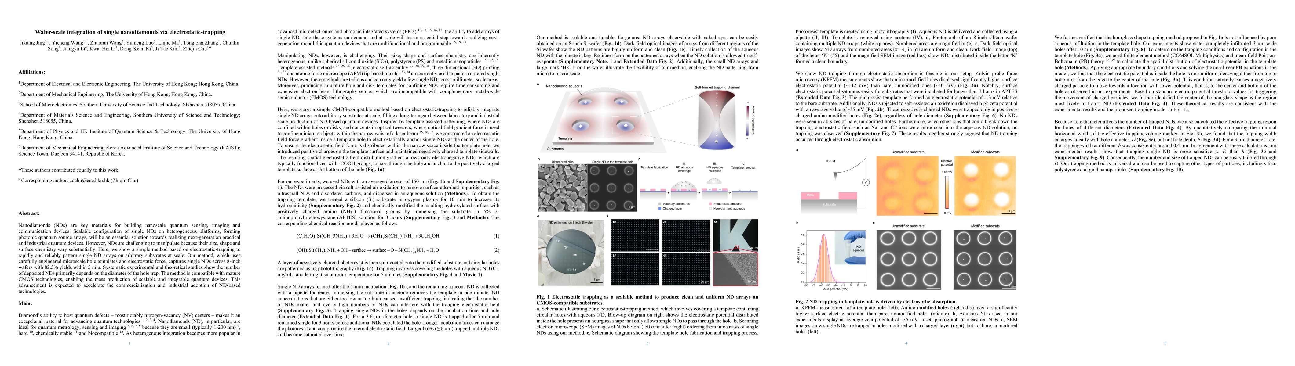
Nanodiamonds (NDs) are key materials for building nanoscale quantum sensing, imaging and communication devices. Scalable configuration of single NDs on heterogeneous platforms, forming photonic quantum source arrays, will be an essential solution towards realizing next-generation practical and industrial quantum devices. However, NDs are challenging to manipulate because their size, shape and surface chemistry vary substantially. Here, we show a simple method based on electrostatic-trapping to rapidly and reliably pattern single ND arrays on arbitrary substrates at scale. Our method, which uses carefully engineered microscale hole templates and electrostatic force, captures single NDs across 8-inch wafers with 82.5% yields within 5 min. Systematic experimental and theoretical studies show the number of deposited NDs primarily depends on the diameter of the hole trap. The method is compatible with mature CMOS technologies, enabling the mass production of scalable and integrable quantum devices. This advancement is expected to accelerate the commercialization and industrial adoption of ND-based technologies.

AI Key Findings

Generated Oct 01, 2025

Methodology — What approach did the authors take?

The research employs electrostatic-trapping using microscale hole templates to pattern single nanodiamonds (NDs) on substrates. The method involves photolithography, electrostatic force, and controlled deposition of NDs through template holes.

Key Results — What are the main findings?

  • Achieved 82.5% yield of single ND arrays on 8-inch wafers within 5 minutes.
  • Trapping efficiency is primarily determined by the diameter of the hole template, with smaller holes leading to fewer deposited NDs and larger holes allowing more deposition.
  • The method is compatible with CMOS technology, enabling scalable integration of NDs on heterogeneous platforms.

Significance — Why does this research matter?

This advancement enables mass production of quantum devices using nanodiamonds, accelerating commercialization of quantum technologies in sensing, imaging, and communication.

Technical Contribution — What is the technical contribution?

Development of a CMOS-compatible electrostatic-trapping technique for precise, large-scale integration of single nanodiamonds on arbitrary substrates.

Novelty — What is new about this work?

The method introduces a simple, highly reproducible electrostatic-trapping mechanism that enables scalable, wafer-level integration of single NDs without complex fabrication steps.

Limitations — What are the limitations of this study?

  • The method's effectiveness is dependent on precise control of template dimensions and electrostatic potential distribution.
  • Long-term trapping may lead to degradation of the photoresist, affecting stability.

Future Work — What did the authors propose for future work?

  • Exploring optimization of hole diameters for different ND sizes and applications.
  • Investigating long-term stability and reliability of trapped NDs in various environments.
  • Expanding the method to other nanomaterials beyond nanodiamonds.

Paper Details

Paper ID: 2509.23032
Categories:
physics.optics

How to Cite This Paper

BibTeX
@article{song2025wafer,
  title         = {Wafer-scale integration of single nanodiamonds via
  electrostatic-trapping},
  author        = {Song, Chunlin and Ki, Dong-Keun and Kim, Ji Tae and others},
  year          = {2025},
  eprint        = {2509.23032},
  archivePrefix = {arXiv},
  primaryClass  = {physics.optics},
}
APA 7
Song, C., Ki, D., Kim, J., Li, J., Jing, J., Li, K., Ma, L., Zhang, T., Wang, Y., Luo, Y., Chu, Z., & Wang, Z. (2025). Wafer-scale integration of single nanodiamonds via
  electrostatic-trapping. arXiv. https://arxiv.org/abs/2509.23032
MLA 9
Song, Chunlin, et al. "Wafer-scale integration of single nanodiamonds via
  electrostatic-trapping." arXiv, 2025, arxiv.org/abs/2509.23032.

Similar Papers

Found 4 papers

Comments (0)

This website uses cookies to ensure you get the best experience. Learn more