John Mucci

5 papers on arXiv

Academic Profile

Name: J. Mucci
Total Papers: 15

Statistics

arXiv Papers 5
Total Publications 15

Papers on arXiv

Thumbnail for Engineering of Niobium Surfaces Through Accelerated Neutral Atom Beam
  Technology For Quantum Applications

Engineering of Niobium Surfaces Through Accelerated Neutral Atom Beam Technology For Quantum Applications

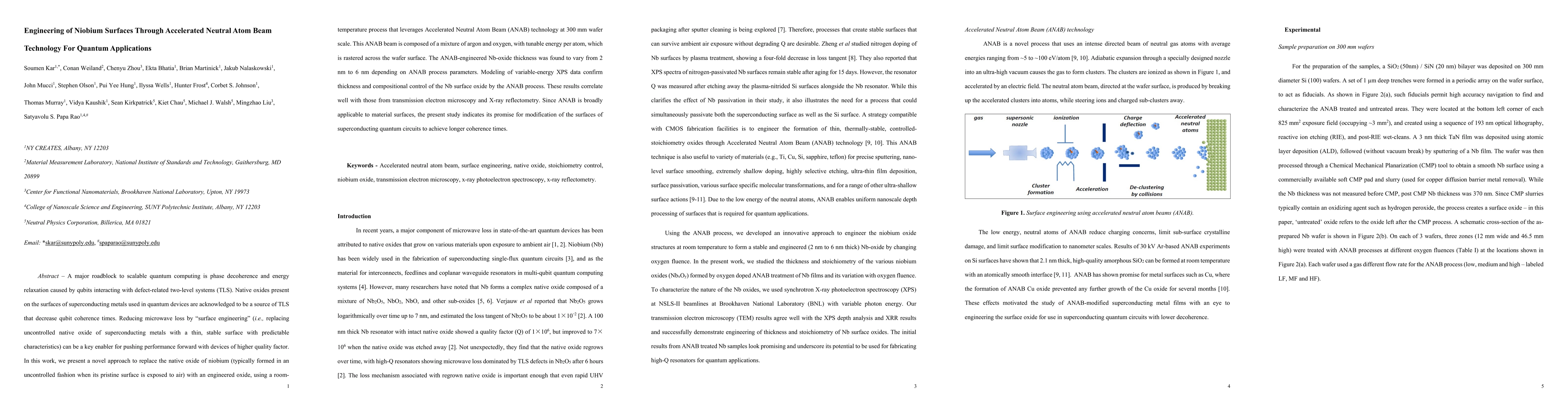
A major roadblock to scalable quantum computing is phase decoherence and energy relaxation caused by qubits interacting with defect-related two-level systems (TLS). Native oxides present on the surf...

Thumbnail for Chemical Mechanical Planarization for Ta-based Superconducting Quantum
  Devices

Chemical Mechanical Planarization for Ta-based Superconducting Quantum Devices

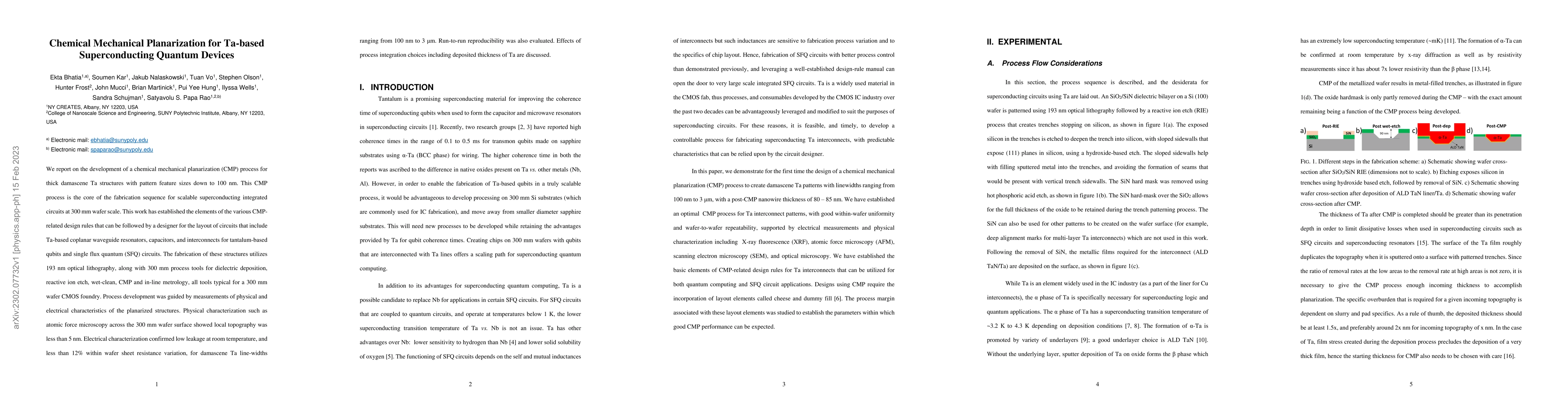
We report on the development of a chemical mechanical planarization (CMP) process for thick damascene Ta structures with pattern feature sizes down to 100 nm. This CMP process is the core of the fab...

Thumbnail for A full degree-of-freedom photonic crystal spatial light modulator

A full degree-of-freedom photonic crystal spatial light modulator

Harnessing the full complexity of optical fields requires complete control of all degrees-of-freedom within a region of space and time -- an open goal for present-day spatial light modulators (SLMs)...

Thumbnail for Ta-based Josephson junctions using insulating ALD TaN tunnel barriers

Ta-based Josephson junctions using insulating ALD TaN tunnel barriers

Josephson junctions form the core circuit element in superconducting quantum computing circuits, single flux quantum digital logic circuits, and sensing devices such as SQUIDs. Aluminum oxide has typi...

Thumbnail for Effects of Integrated Heatsinking on Superconductivity in Tantalum Nitride Nanowires at the 300 Millimeter Scale

Effects of Integrated Heatsinking on Superconductivity in Tantalum Nitride Nanowires at the 300 Millimeter Scale

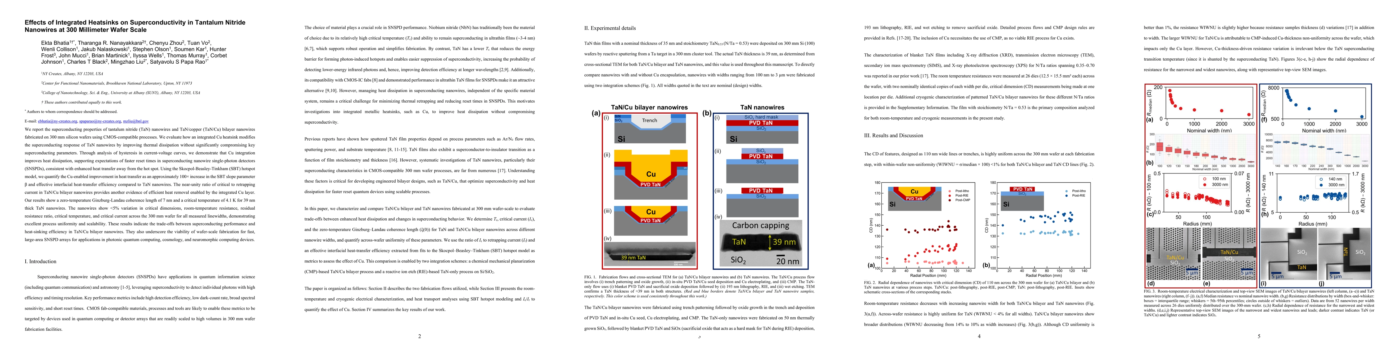
We report the superconducting properties of tantalum nitride (TaN) nanowires and TaN/copper (TaN/Cu) bilayer nanowires fabricated on 300 mm silicon wafers using CMOS-compatible processes. We evaluate ...

This website uses cookies to ensure you get the best experience. Learn more