Chemical Mechanical Planarization for Ta-based Superconducting Quantum Devices
Publication
Metrics
AI Quick Summary
This paper details the development of a chemical mechanical planarization (CMP) process for fabricating Ta-based superconducting quantum devices, achieving feature sizes down to 100 nm. The CMP process is essential for scalable superconducting integrated circuits, ensuring low leakage and minimal topography variation across 300 mm wafers.
Paper Preview
Abstract
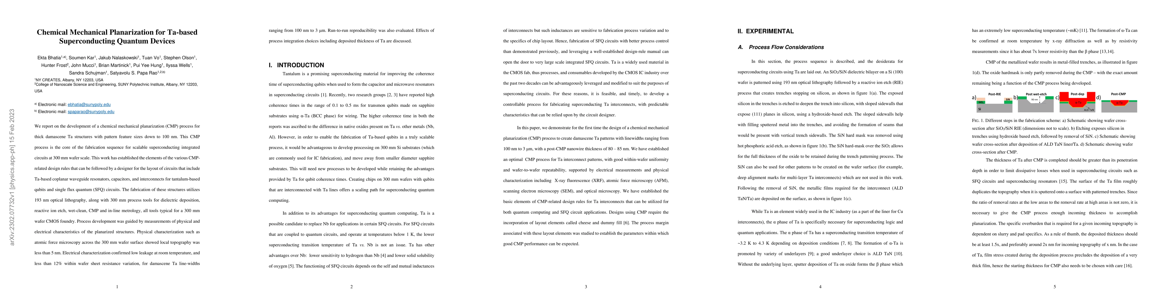
We report on the development of a chemical mechanical planarization (CMP) process for thick damascene Ta structures with pattern feature sizes down to 100 nm. This CMP process is the core of the fabrication sequence for scalable superconducting integrated circuits at 300 mm wafer scale. This work has established the elements of the various CMP-related design rules that can be followed by a designer for the layout of circuits that include Ta-based coplanar waveguide resonators, capacitors, and interconnects for tantalum-based qubits and single flux quantum (SFQ) circuits. The fabrication of these structures utilizes 193 nm optical lithography, along with 300 mm process tools for dielectric deposition, reactive ion etch, wet-clean, CMP and in-line metrology, all tools typical for a 300 mm wafer CMOS foundry. Process development was guided by measurements of physical and electrical characteristics of the planarized structures. Physical characterization such as atomic force microscopy across the 300 mm wafer surface showed local topography was less than 5 nm. Electrical characterization confirmed low leakage at room temperature, and less than 12% within wafer sheet resistance variation, for damascene Ta line-widths ranging from 100 nm to 3 {\mu}m. Run-to-run reproducibility was also evaluated. Effects of process integration choices including deposited thickness of Ta are discussed.
AI Key Findings
Get AI-generated insights about this paper's methodology, results, significance, and more — seven facets brought into focus.
Impact
Paper Details
Authors
PDF Preview
Key Terms
Citation Network
Current paper (gray), citations (green), references (blue)
Display is limited for performance on very large graphs.
Discussion 0