Academic Profile
Statistics
Similar Authors
Papers on arXiv
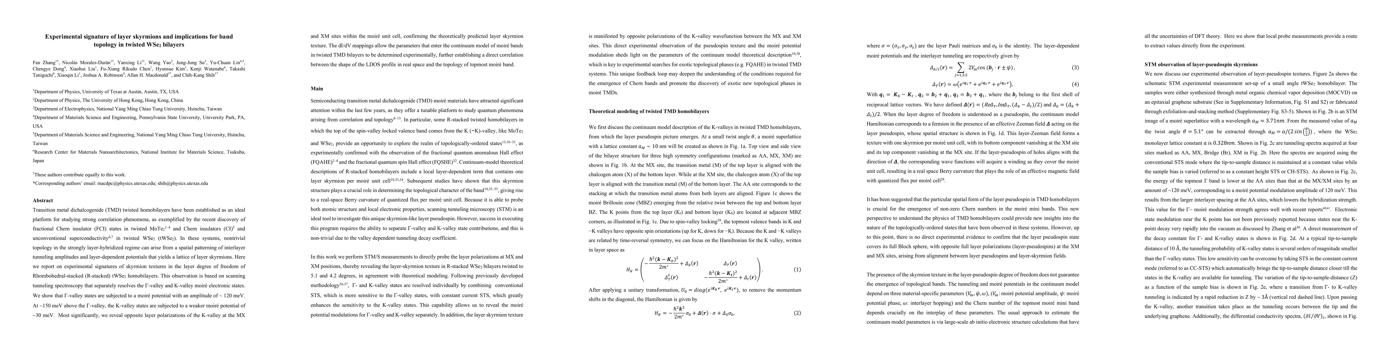
Transition metal dichalcogenide (TMD) twisted homobilayers have been established as an ideal platform for studying strong correlation phenomena, as exemplified by the recent discovery of fractional ...
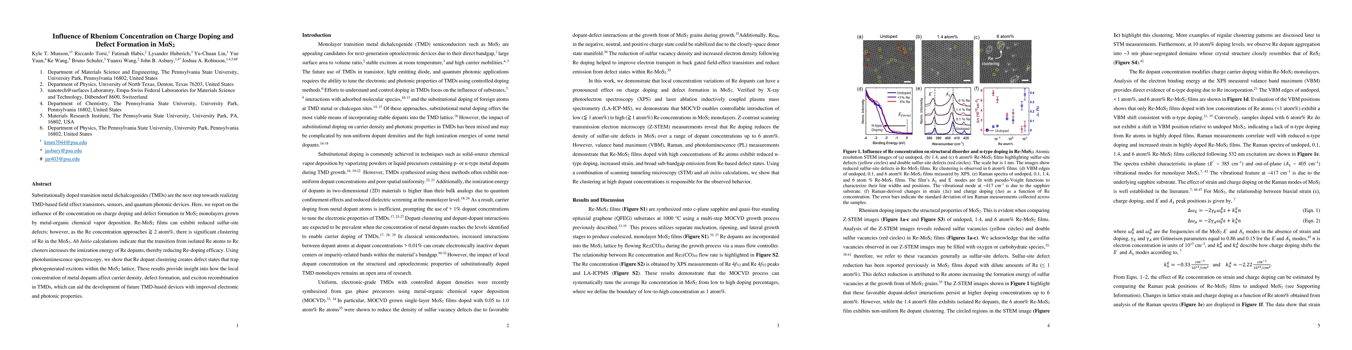
Substitutionally doped transition metal dichalcogenides (TMDs) are the next step towards realizing TMD-based field effect transistors, sensors, and quantum photonic devices. Here, we report on the i...
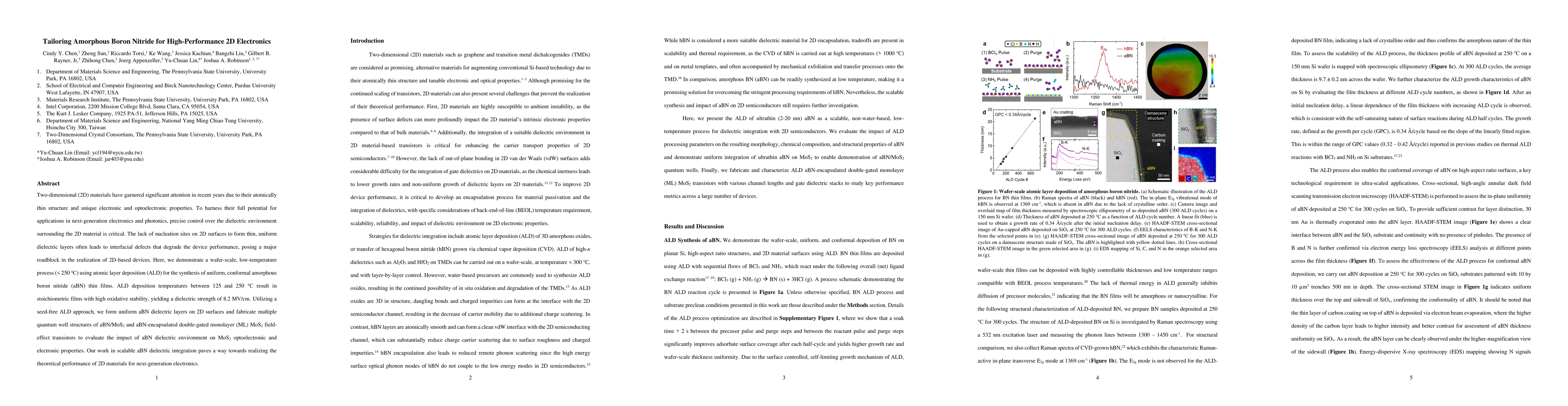
Two-dimensional (2D) materials have garnered significant attention in recent years due to their atomically thin structure and unique electronic and optoelectronic properties. To harness their full p...
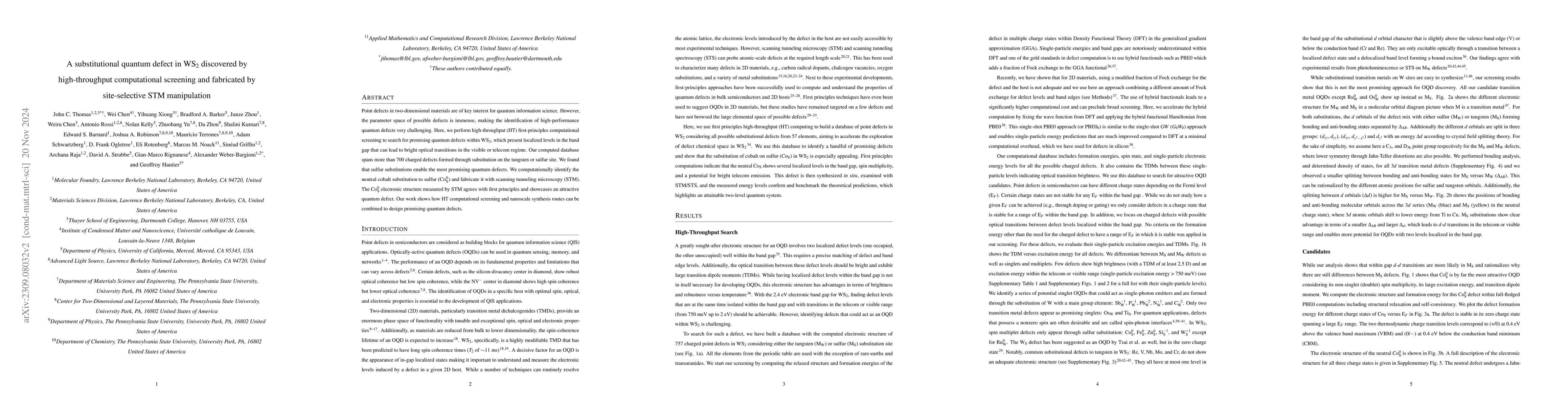
Point defects in two-dimensional materials are of key interest for quantum information science. However, the space of possible defects is immense, making the identification of high-performance quant...
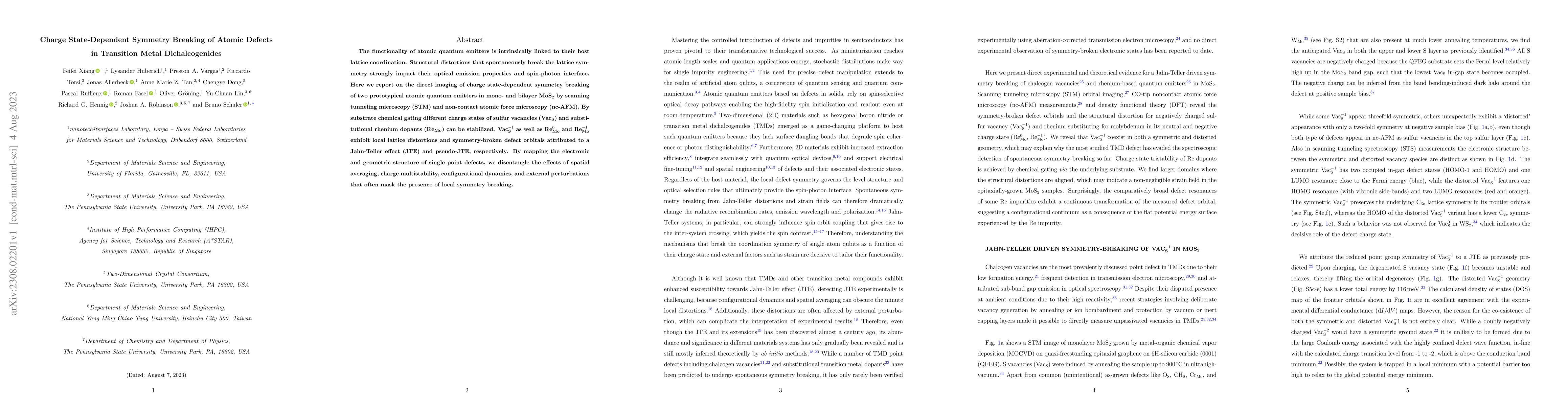
The functionality of atomic quantum emitters is intrinsically linked to their host lattice coordination. Structural distortions that spontaneously break the lattice symmetry strongly impact their op...
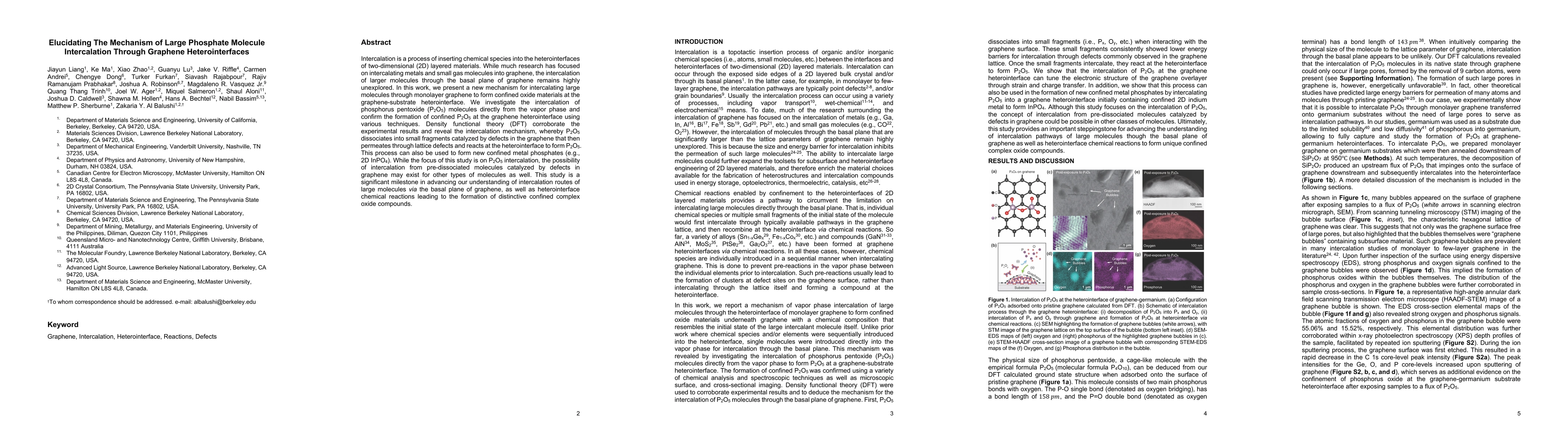
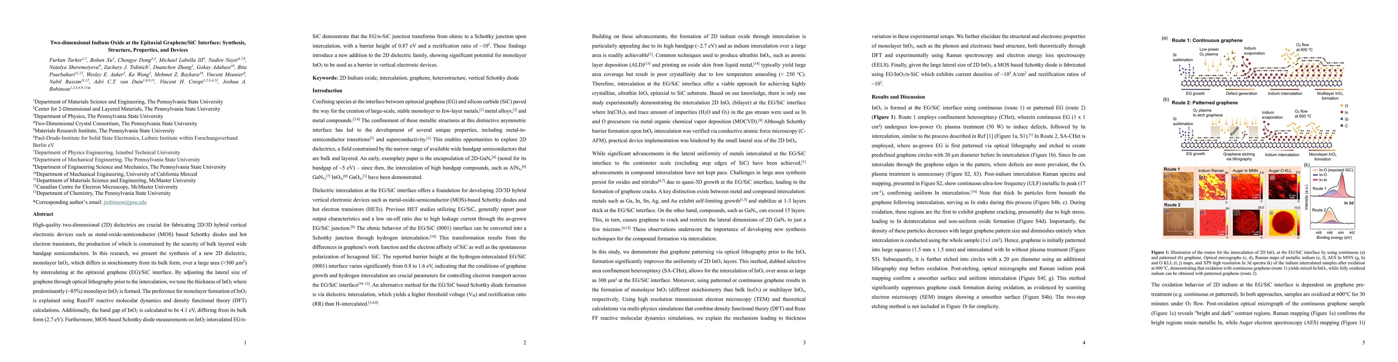
Intercalation is a process of inserting chemical species into the heterointerfaces of two-dimensional (2D) layered materials. While much research has focused on intercalating metals and small gas mo...
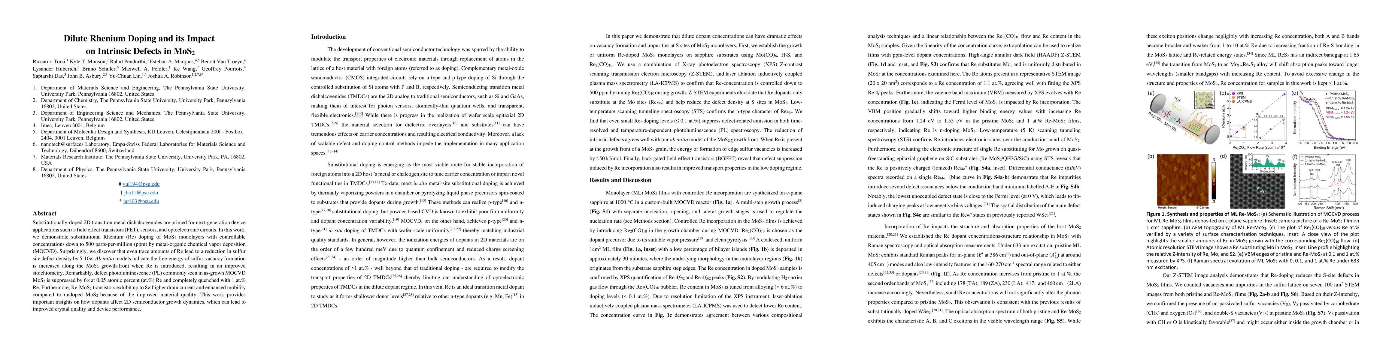
Substitutionally-doped 2D transition metal dichalcogenides are primed for next-generation device applications such as field effect transistors (FET), sensors, and optoelectronic circuits. In this wo...
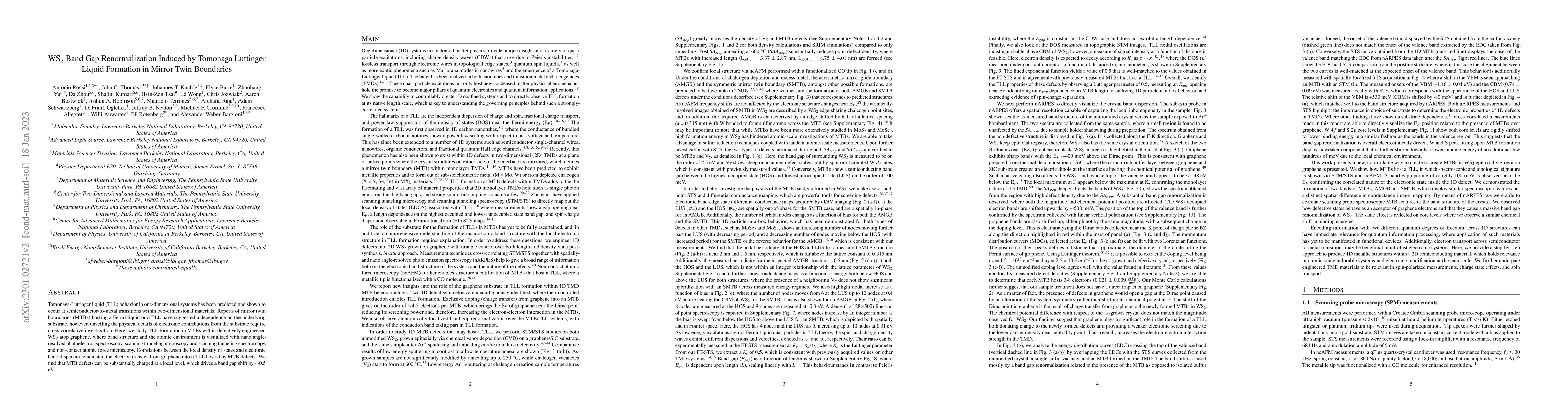
Tomonaga-Luttinger liquid (TLL) behavior in one-dimensional systems has been predicted and shown to occur at semiconductor-to-metal transitions within two-dimensional materials. Reports of mirror tw...
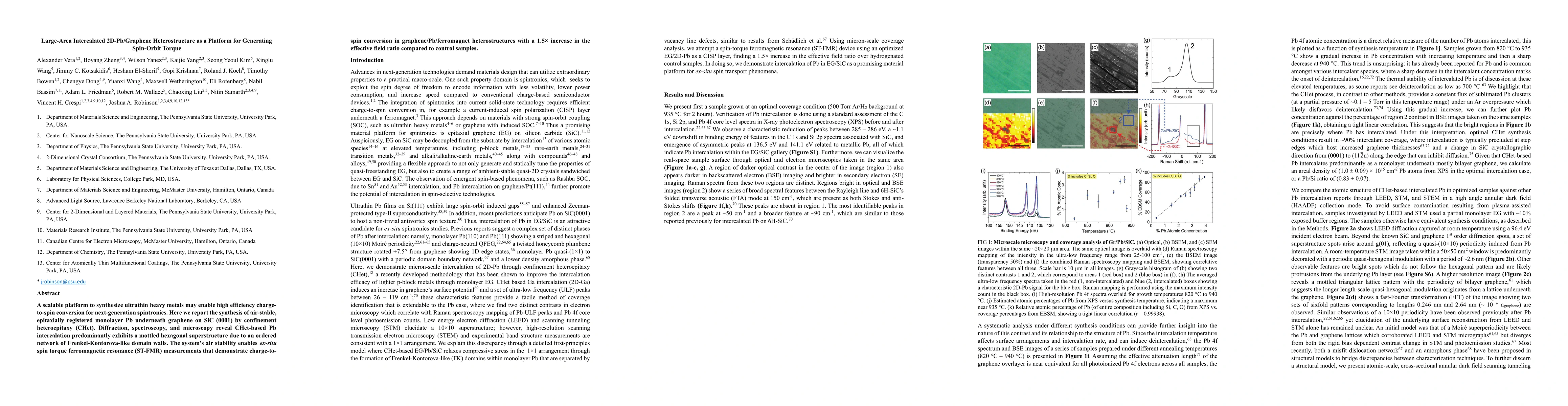
A scalable platform to synthesize ultrathin heavy metals may enable high efficiency charge-to-spin conversion for next-generation spintronics. Here we report centimeter-scale synthesis of air-stable...

The introduction of superconductivity to the Dirac surface states of a topological insulator leads to a topological superconductor, which may support topological quantum computing through Majorana z...
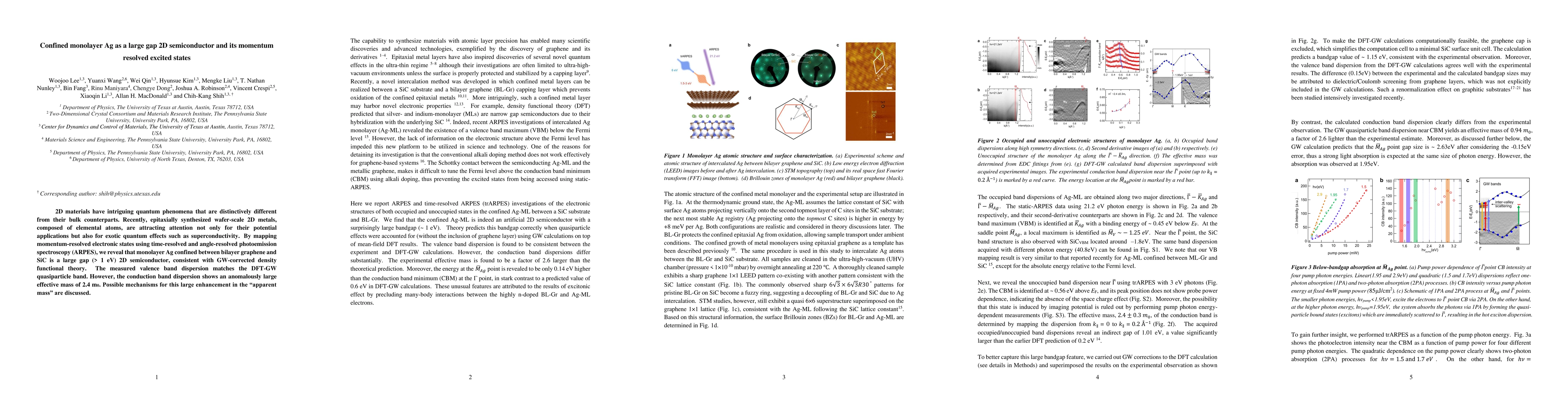
2D materials have intriguing quantum phenomena that are distinctively different from their bulk counterparts. Recently, epitaxially synthesized wafer-scale 2D metals, composed of elemental atoms, ar...
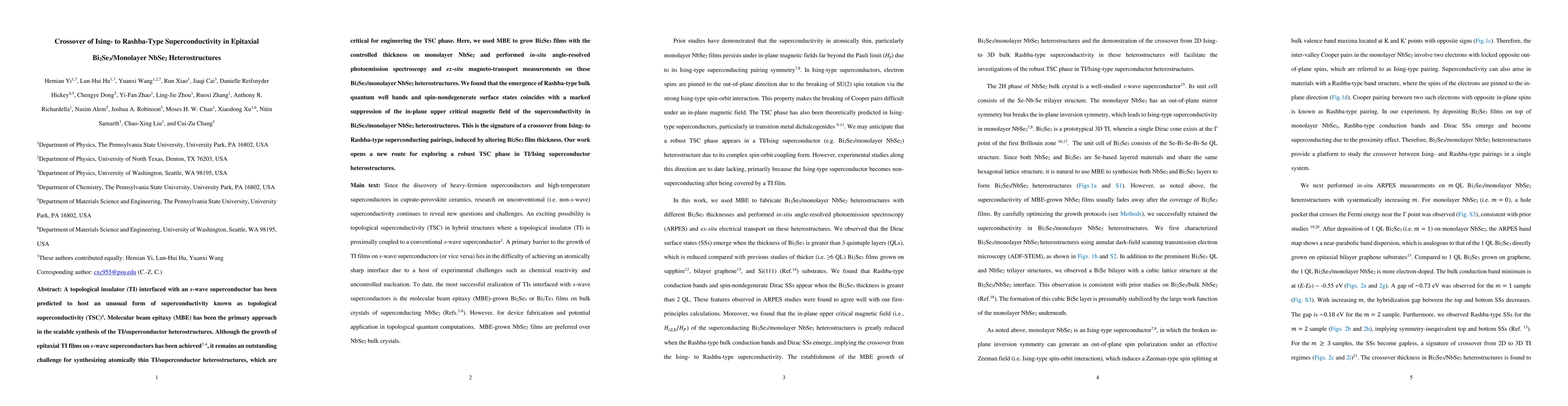
A topological insulator (TI) interfaced with an s-wave superconductor has been predicted to host an unusual form of superconductivity known as topological superconductivity (TSC). Molecular beam epi...
Semiconducting two-dimensional (2D) transition metal dichalcogenides (TMDs) are considered a key materials class to scale microelectronics to the ultimate atomic level. The robust quantum properties...
Individual atomic defects in 2D materials impact their macroscopic functionality. Correlating the interplay is challenging, however, intelligent hyperspectral scanning tunneling spectroscopy (STS) m...
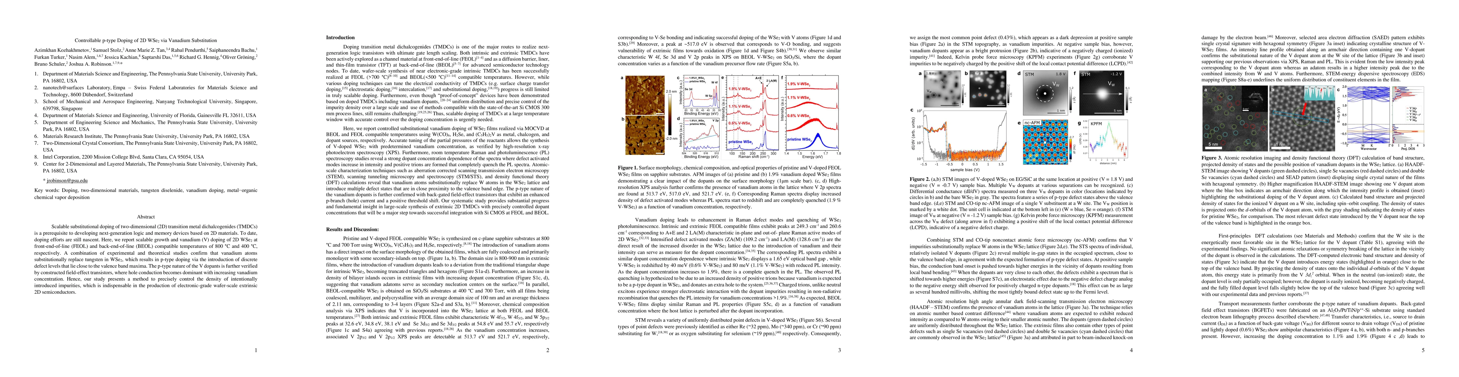
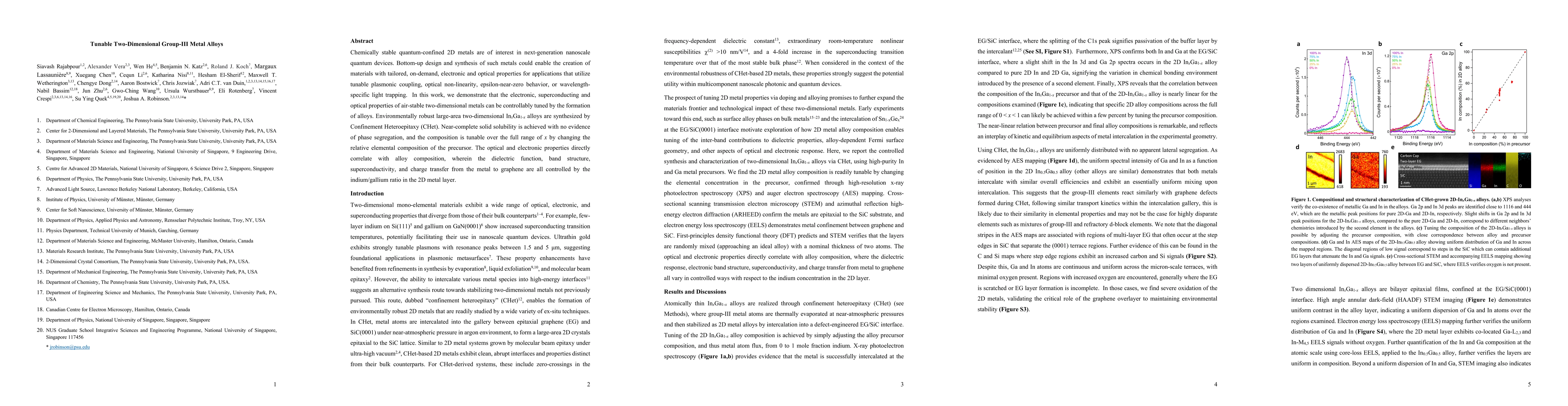
Scalable substitutional doping of two-dimensional (2D) transition metal dichalcogenides (TMDCs) is a prerequisite to developing next-generation logic and memory devices based on 2D materials. To dat...
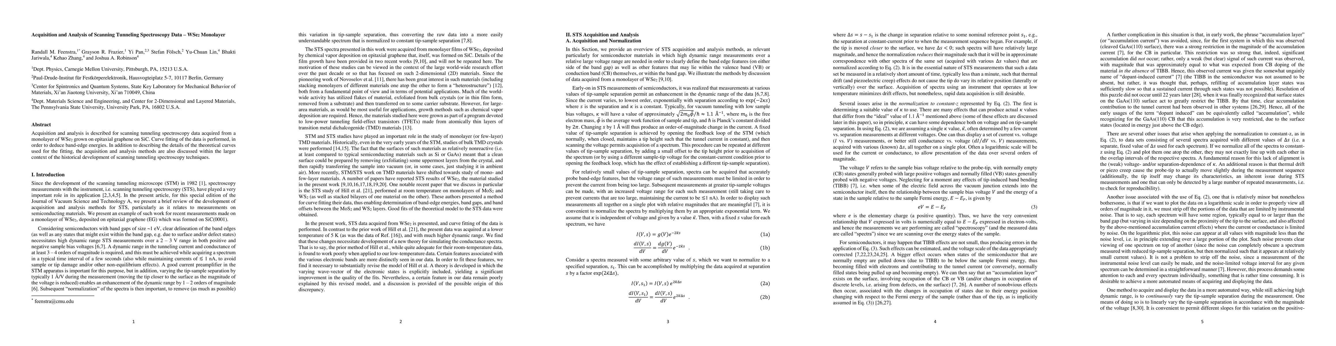
Chemically stable quantum-confined 2D metals are of interest in next-generation nanoscale quantum devices. Bottom-up design and synthesis of such metals could enable the creation of materials with t...
Acquisition and analysis is described for scanning tunneling spectroscopy data acquired from a monolayer of WSe$_2$ grown on epitaxial graphene on SiC. Curve fitting of the data is performed, in ord...
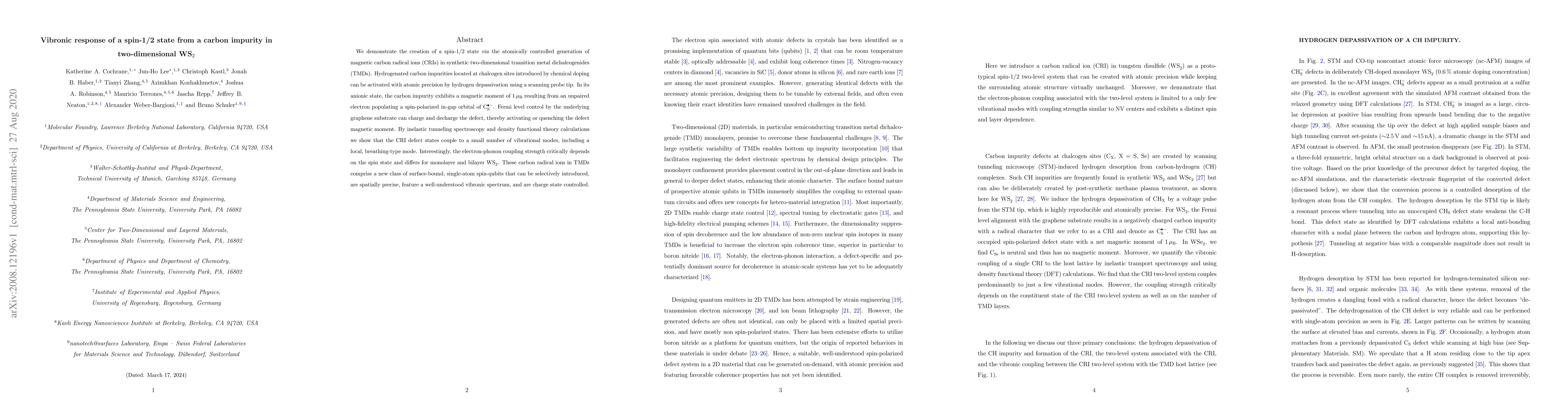
We demonstrate the creation of a spin-1/2 state via the atomically controlled generation of magnetic carbon radical ions (CRIs) in synthetic two-dimensional transition metal dichalcogenides (TMDs). ...
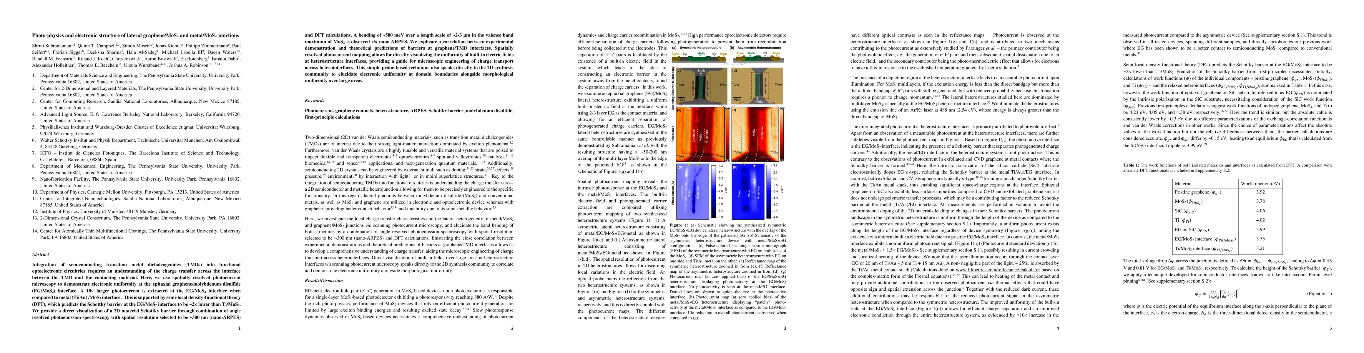
Integration of semiconducting transition metal dichalcogenides (TMDs) into functional optoelectronic circuitries requires an understanding of the charge transfer across the interface between the TMD...
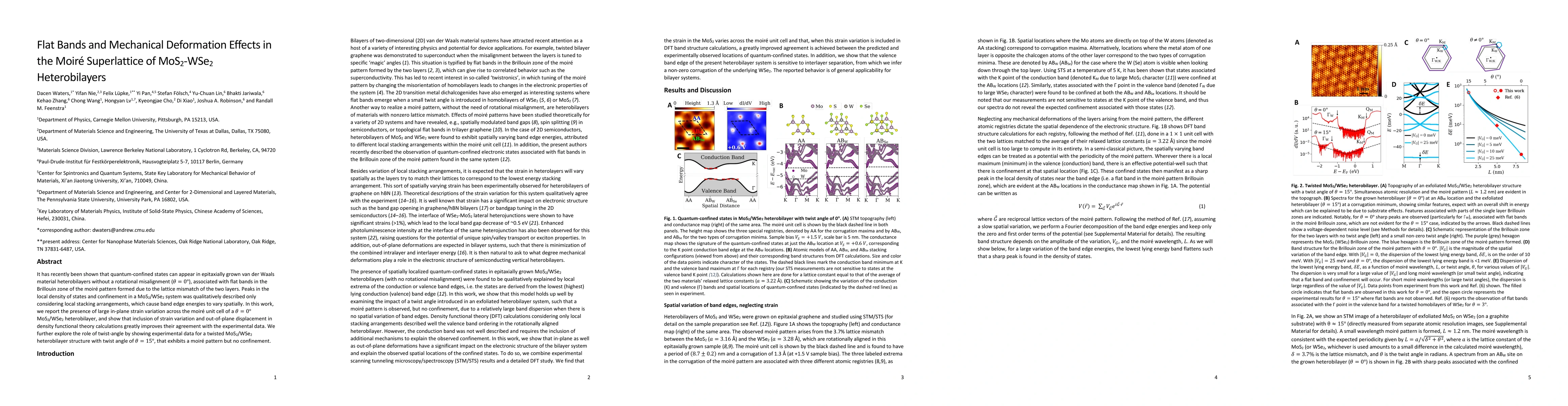
It has recently been shown that quantum-confined states can appear in epitaxially grown van der Waals material heterobilayers without a rotational misalignment ($\theta=0^\circ$), associated with fl...
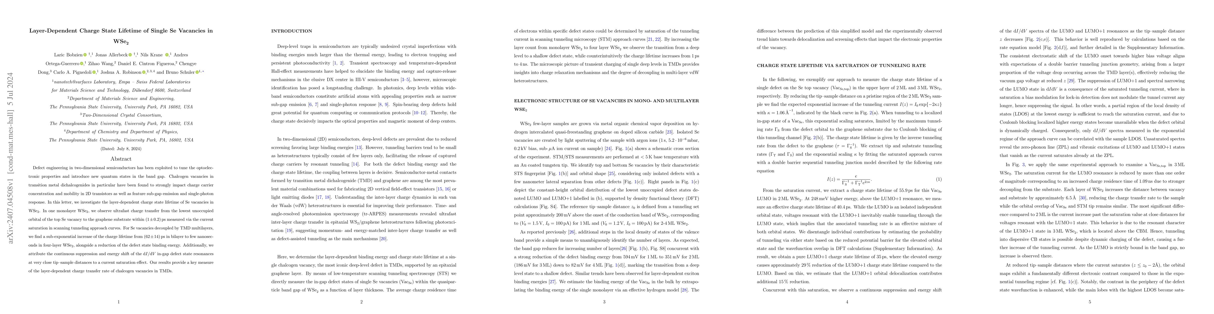
Defect engineering in two-dimensional semiconductors has been exploited to tune the optoelectronic properties and introduce new quantum states in the band gap. Chalcogen vacancies in transition metal ...
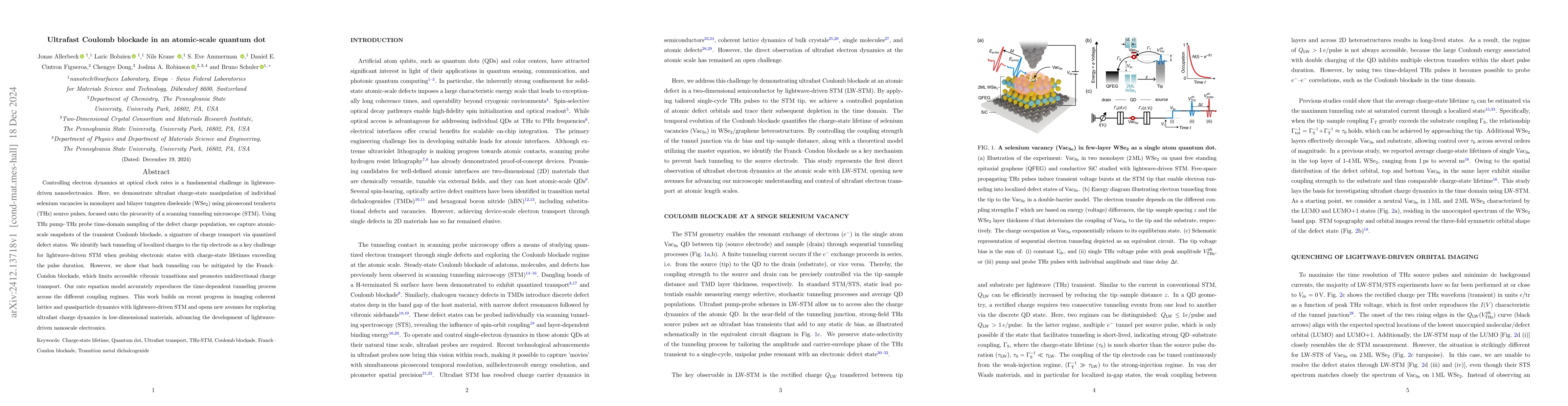
Controlling electron dynamics at optical clock rates is a fundamental challenge in lightwave-driven nanoelectronics. Here, we demonstrate ultrafast charge-state manipulation of individual selenium vac...
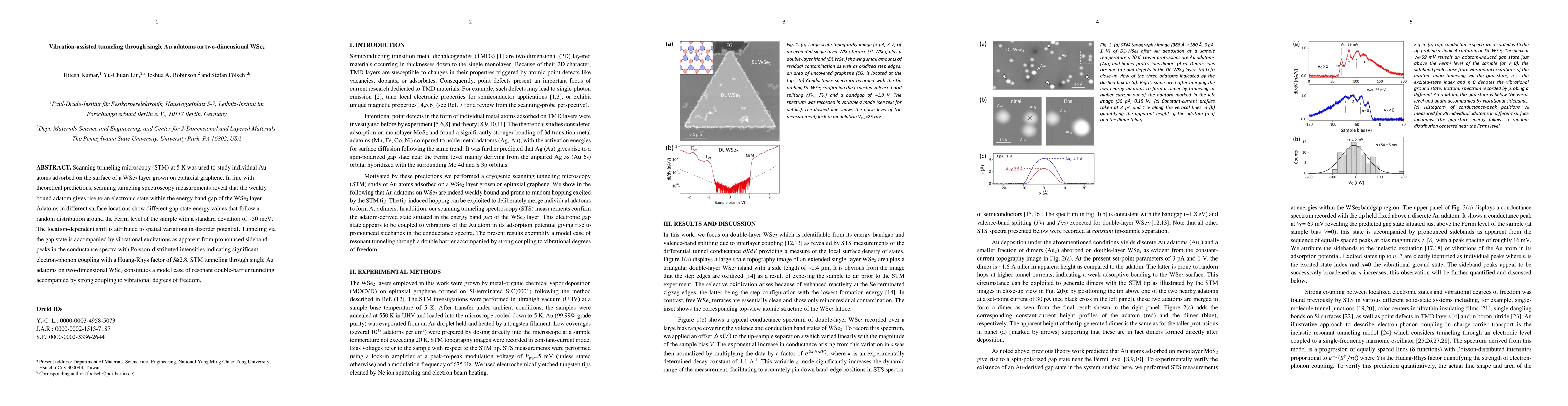
Scanning tunneling microscopy (STM) at 5 K was used to study individual Au atoms adsorbed on the surface of a WSe2 layer grown on epitaxial graphene. In line with theoretical predictions, scanning tun...
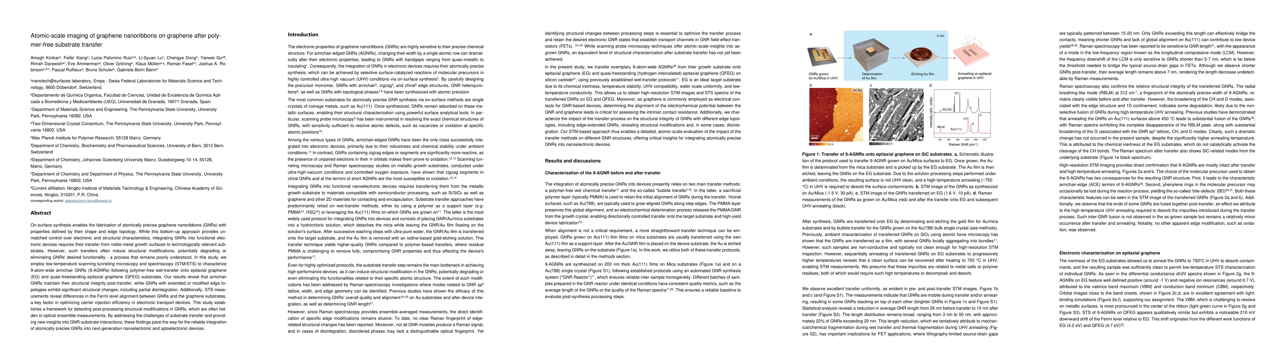
On-surface synthesis enables the fabrication of atomically precise graphene nanoribbons (GNRs) with properties defined by their shape and edge topology. While this bottom-up approach provides unmatche...
High-quality two-dimensional (2D) dielectrics are crucial for fabricating 2D/3D hybrid vertical electronic devices such as metal-oxide-semiconductor (MOS) based Schottky diodes and hot electron transi...
In low-dimensional superconductors, the interplay between quantum confinement and interfacial hybridization effects can reshape Cooper pair wavefunctions and induce novel forms of unconventional super...
Understanding interfacial interactions in two-dimensional (2D) heterostructures is essential for advancing optoelectronic and quantum technologies. We investigate metal-organic chemical vapor depositi...
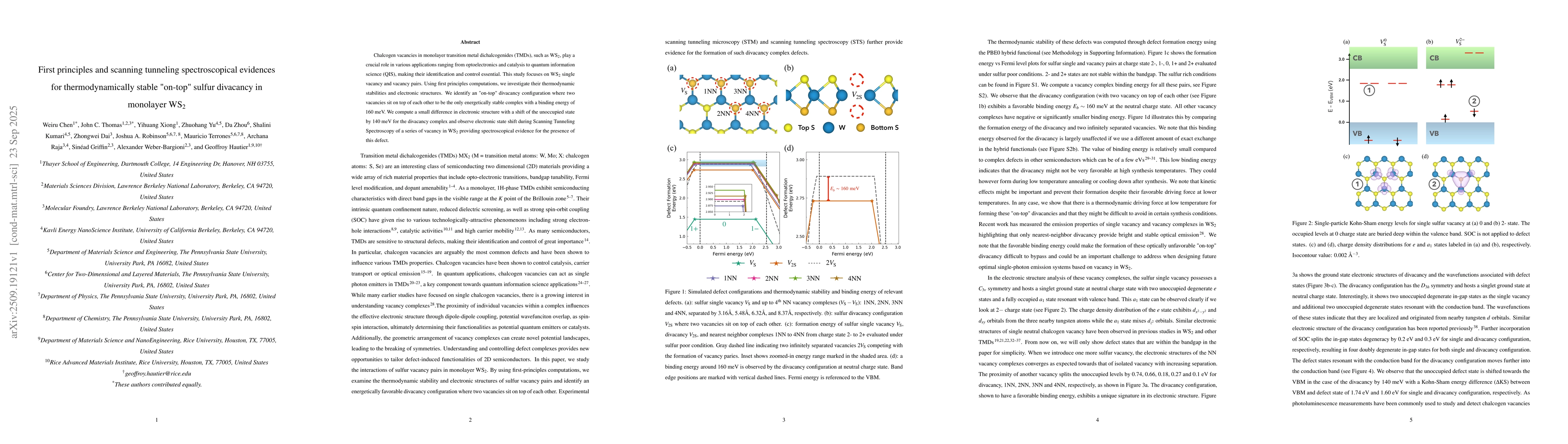
Chalcogen vacancies in monolayer transition metal dichalcogenides (TMDs), such as WS$_{2}$, play a crucial role in various applications ranging from optoelectronics and catalysis to quantum informatio...
Understanding how atomic defects shape the nanoscale optical properties of two-dimensional (2D) semiconductors is essential for advancing quantum technologies and optoelectronics. Using scanning tunne...
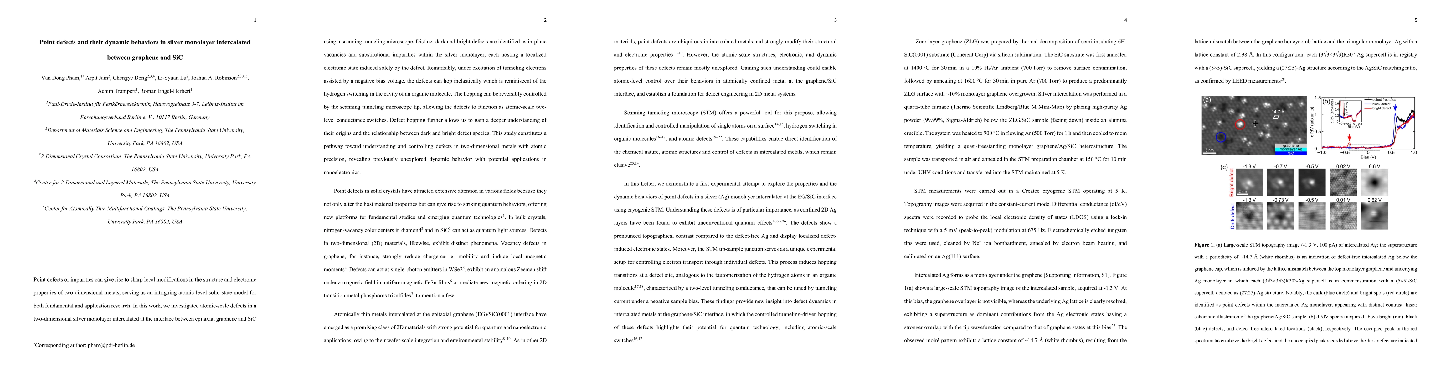
Point defects or impurities can give rise to sharp local modifications in the structure and electronic properties of two-dimensional metals, serving as an intriguing atomic-level solid-state model for...
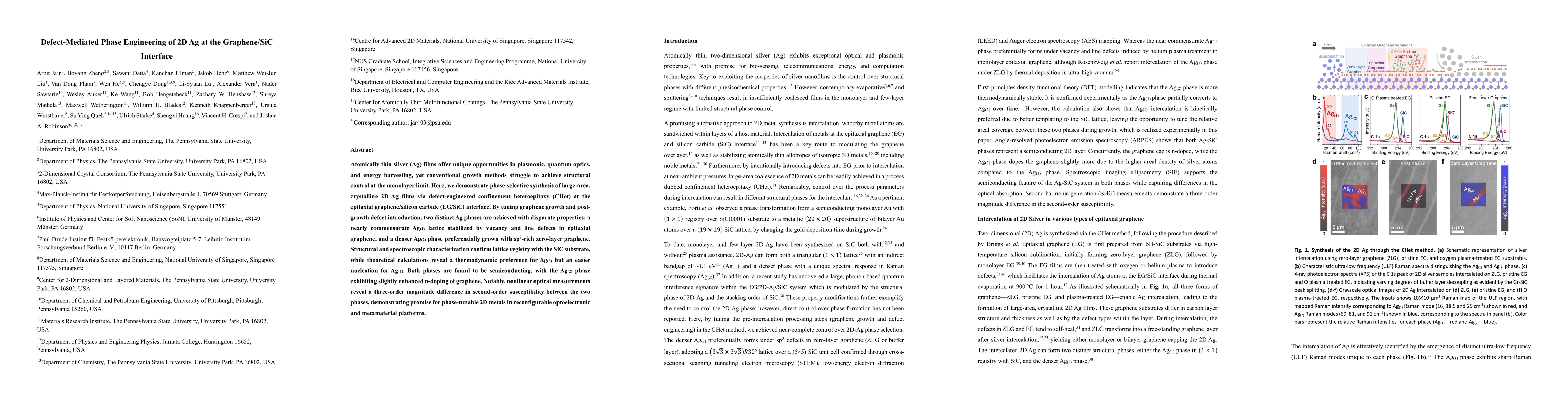
Atomically thin silver (Ag) films offer unique opportunities in plasmonic, quantum optics, and energy harvesting, yet conventional growth methods struggle to achieve structural control at the monolaye...
Motivated by recent studies on superconducting (SC) diode nonreciprocity, we uncover an unexpected hierarchy of SC-phase decoherence in bilayer superconductors hosting both interlayer Josephson coupli...
We demonstrate, by femtosecond time- and angle-resolved photoemission spectroscopy, that photoinduced interlayer charge transfer in a heterostructure consisting of Bernal-stacked bilayer graphene and ...
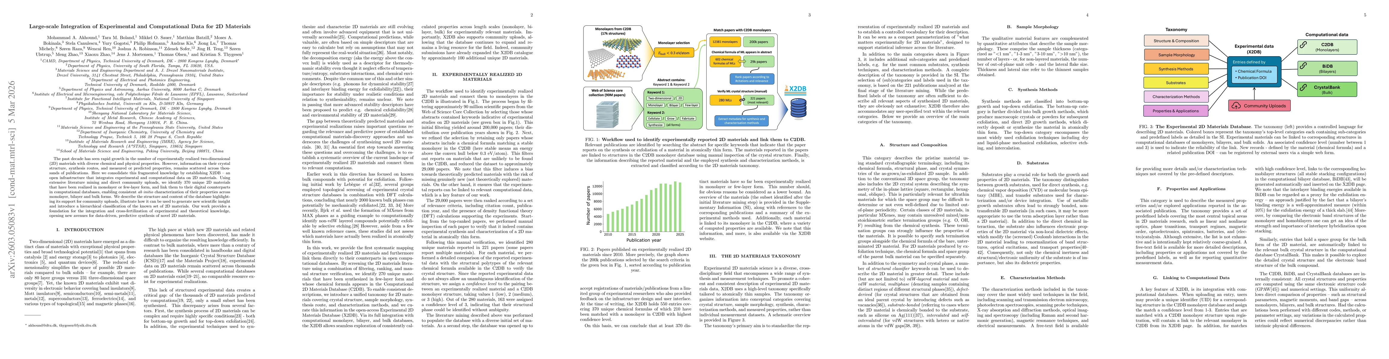
The past decade has seen rapid growth in the number of experimentally realized two-dimensional (2D) materials with diverse chemical and physical properties. However, information on their crystal struc...
Graphene is widely recognized for its ultrafast and broadband photocurrent response, but whether the broadband ultrafast characteristics are preserved at mid-infrared wavelengths with photon energies ...
Collective quantum states are often associated with extended systems, where spatially extensive degrees of freedom enable emergent many-body behavior; whether such strongly correlated states survive a...
Light scattering by two-dimensional (2D) van der Waals heterostructures (vdWHs) is immense, especially given their infinitesimal volume, thus enabling strong light-matter interactions. Surface 2D pola...
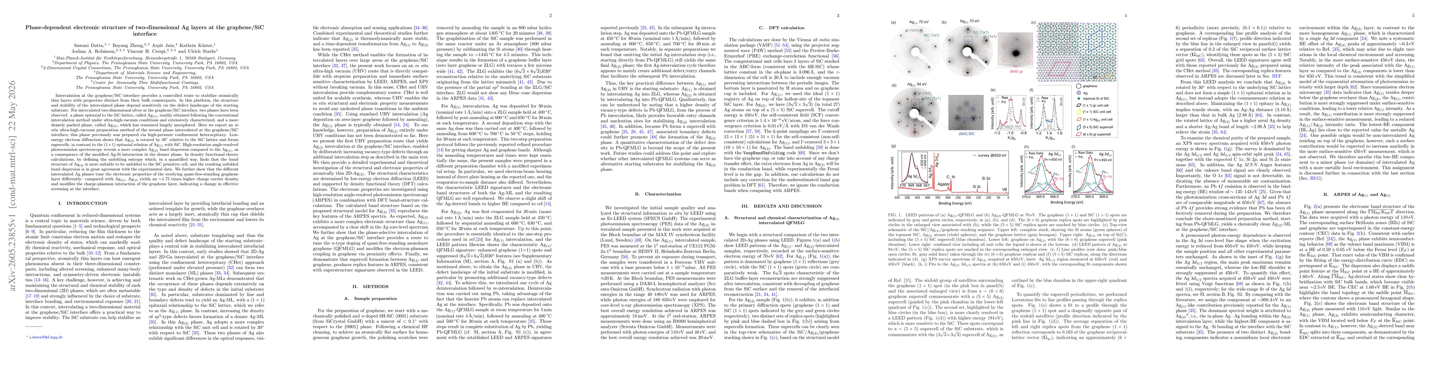
Intercalation at the graphene/SiC interface provides a controlled route to stabilize atomically thin layers with properties distinct from their bulk counterparts. In this platform, the structure and s...