Point defects and their dynamic behaviors in silver monolayer intercalated between graphene and SiC
Publication
Metrics
Paper Preview
Abstract
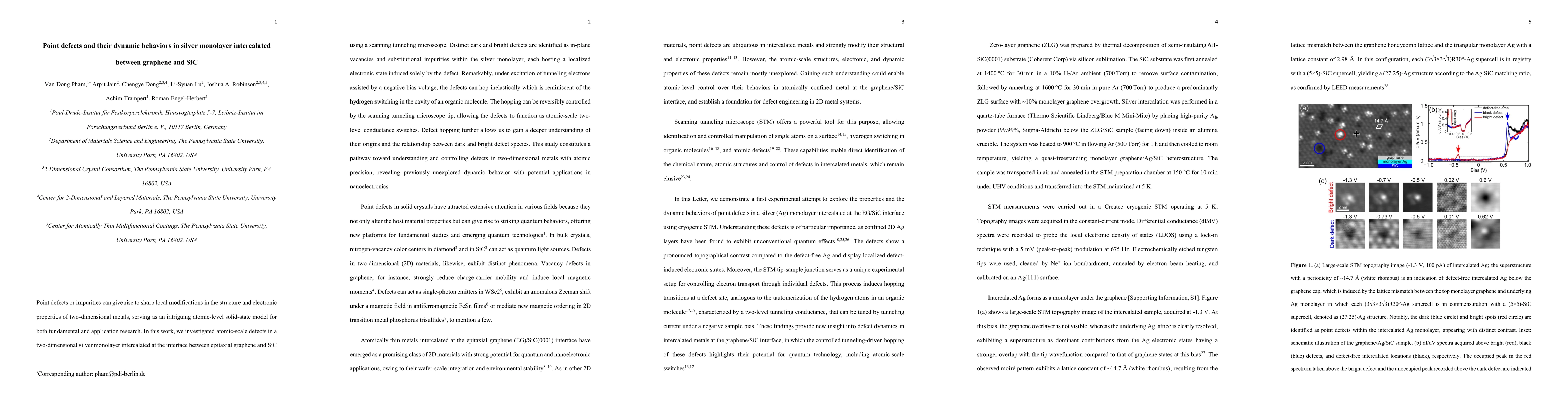
Point defects or impurities can give rise to sharp local modifications in the structure and electronic properties of two-dimensional metals, serving as an intriguing atomic-level solid-state model for both fundamental and application research. In this work, we investigated atomic-scale defects in a two-dimensional silver monolayer intercalated at the interface between epitaxial graphene and SiC using a scanning tunneling microscope. Distinct dark and bright defects are identified as in-plane vacancies and substitutional impurities within the silver monolayer, each hosting a localized electronic state induced solely by the defect. Remarkably, under excitation of tunneling electrons assisted by a negative bias voltage, the defects can hop inelastically which is reminiscent of the hydrogen switching in the cavity of an organic molecule. The hopping can be reversibly controlled by the scanning tunneling microscope tip, allowing the defects to function as atomic-scale two-level conductance switches. Defect hopping further allows us to gain a deeper understanding of their origins and the relationship between dark and bright defect species. This study constitutes a pathway toward understanding and controlling defects in two-dimensional metals with atomic precision, revealing previously unexplored dynamic behavior with potential applications in nanoelectronics.
AI Key Findings
Get AI-generated insights about this paper's methodology, results, significance, and more — seven facets brought into focus.
Discussion 0