Academic Profile
Statistics
Similar Authors
Papers on arXiv
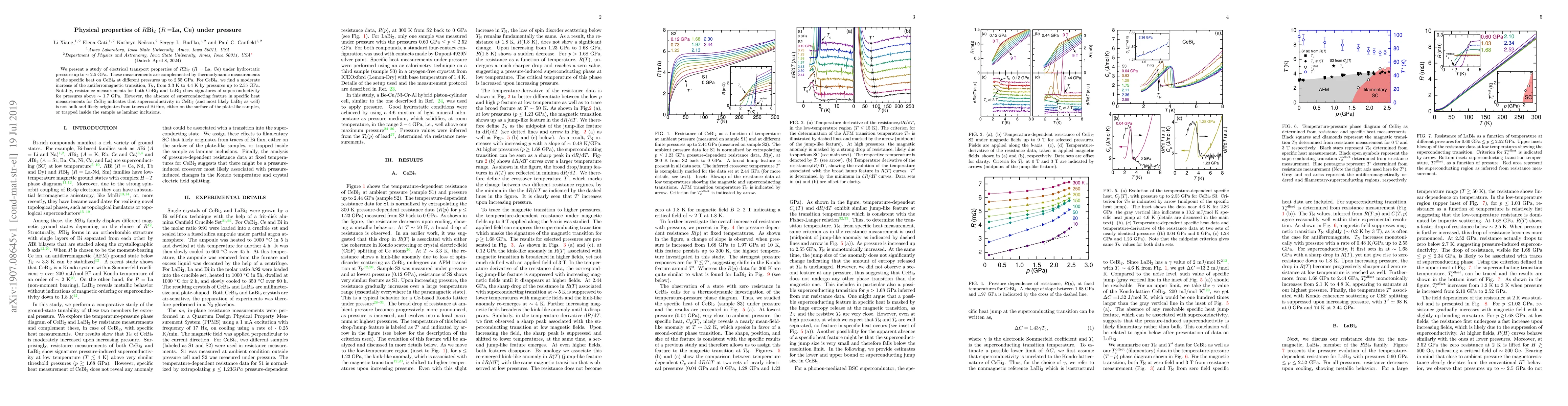
We present a study of electrical transport properties of $R$Bi$_2$ ($R$ = La, Ce) under hydrostatic pressure up to $\sim$ 2.5 GPa. These measurements are complemented by thermodynamic measurements o...
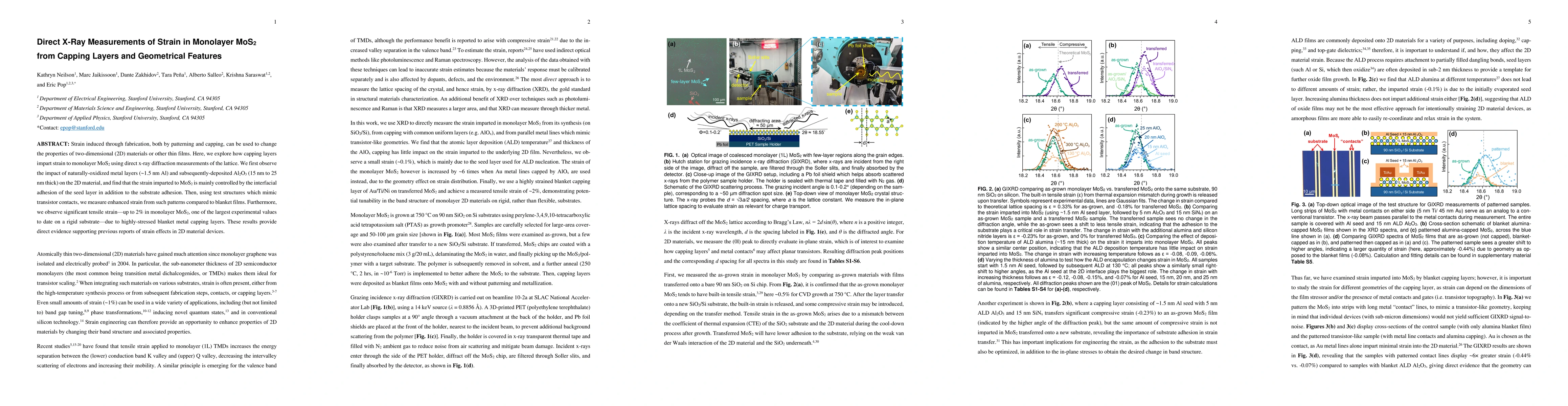
Strain induced through fabrication, both by patterning and capping, can be used to change the properties of two-dimensional (2D) materials or other thin films. Here, we explore how capping layers impa...
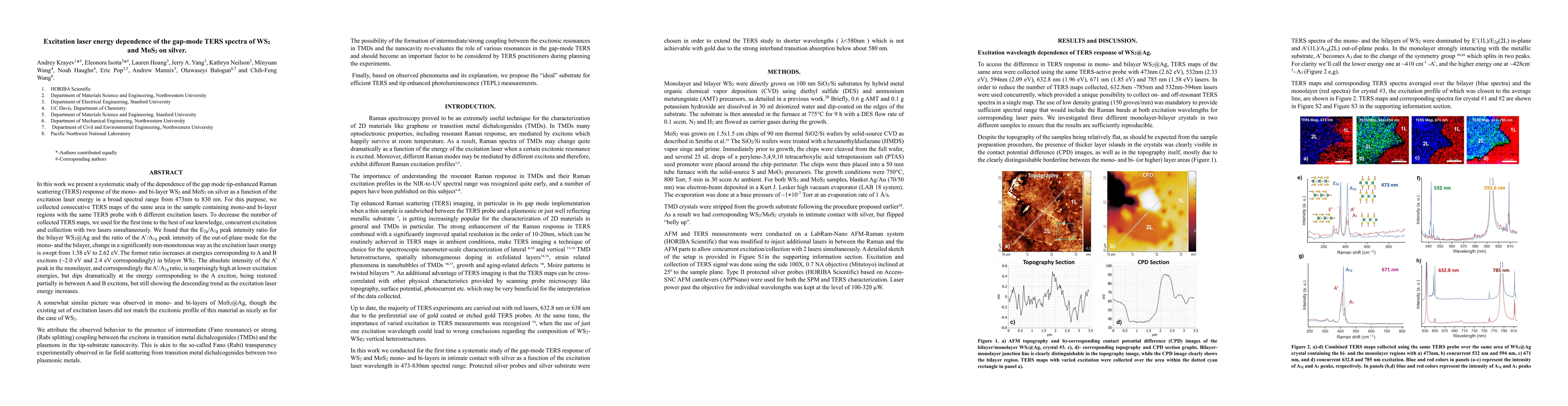
We present a systematic study of the dependence of gap mode tip-enhanced Raman scattering (TERS) of mono- and bi-layer WS$_2$ and MoS$_2$ as a function of excitation laser energy. We collected consecu...
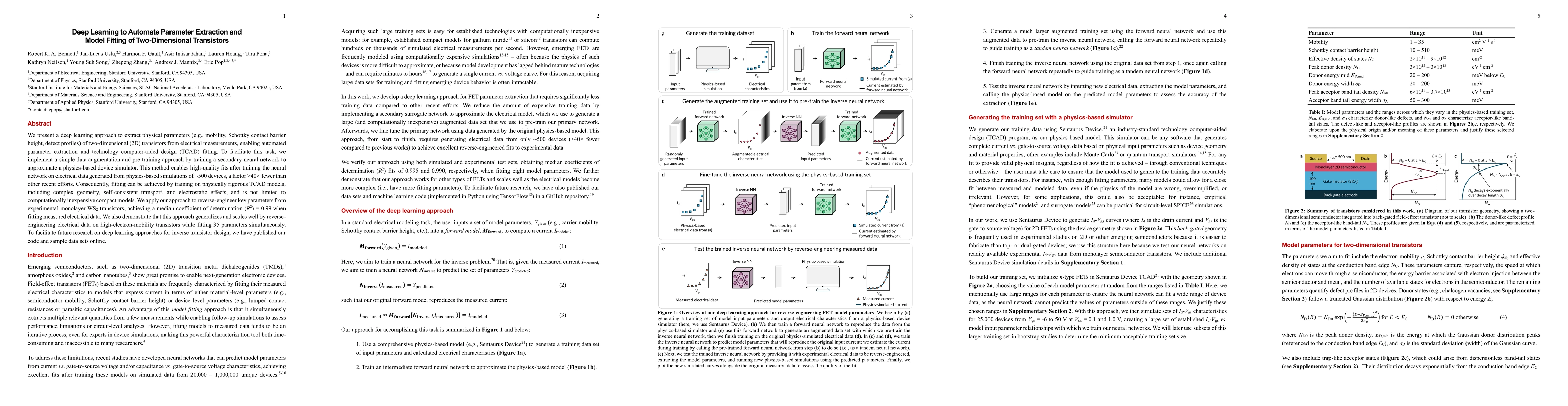
We present a deep learning approach to extract physical parameters (e.g., mobility, Schottky contact barrier height, defect profiles) of two-dimensional (2D) transistors from electrical measurements, ...
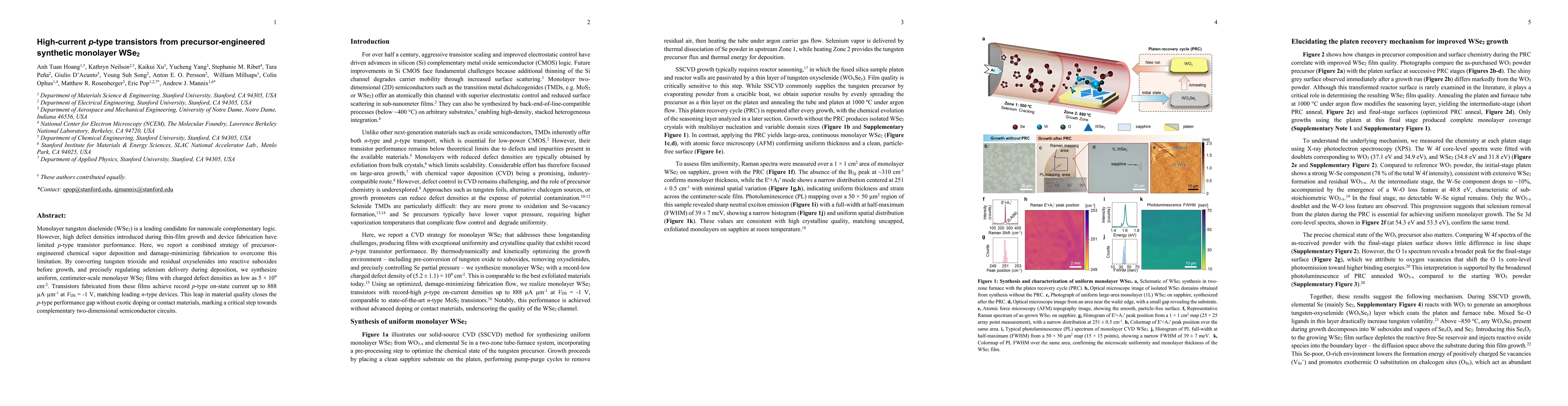
Monolayer tungsten diselenide (WSe$_2$) is a leading candidate for nanoscale complementary logic. However, high defect densities introduced during thin-film growth and device fabrication have limited ...
Nanoscale transistors require aggressive reduction of all channel dimensions: length, width, and thickness. While monolayer two-dimensional semiconductors (2DS) offer ultimate thickness scaling, good ...