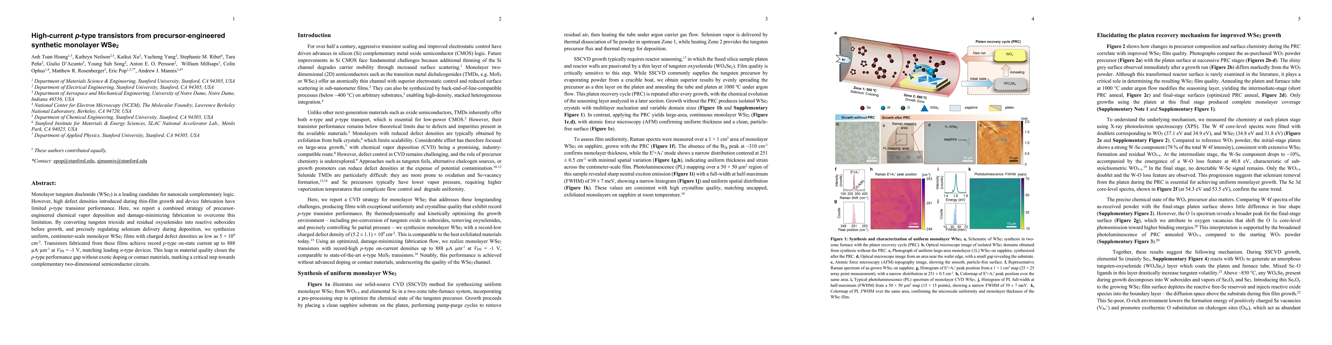
Monolayer tungsten diselenide (WSe$_2$) is a leading candidate for nanoscale
complementary logic. However, high defect densities introduced during thin-film
growth and device fabrication have limited p-type transistor performance. Here,
we report a combined strategy of precursor-engineered chemical vapor deposition
and damage-minimizing fabrication to overcome this limitation. By converting
tungsten trioxide and residual oxyselenides into reactive suboxides before
growth, and precisely regulating selenium delivery during deposition, we
synthesize uniform, centimeter-scale monolayer WSe$_2$ films with charged
defect densities as low as $5 \times 10^{9}$ cm$^{-2}$. Transistors fabricated
from these films achieve record p-type on-state current up to $888
\mu$A$\cdot\mu$m$^{-1}$ at $V_{\mathrm{DS}}=-1$ V, matching leading n-type
devices. This leap in material quality closes the p-type performance gap
without exotic doping or contact materials, marking a critical step towards
complementary two-dimensional semiconductor circuits.
Discussion 0