Academic Profile
Statistics
Similar Authors
Papers on arXiv
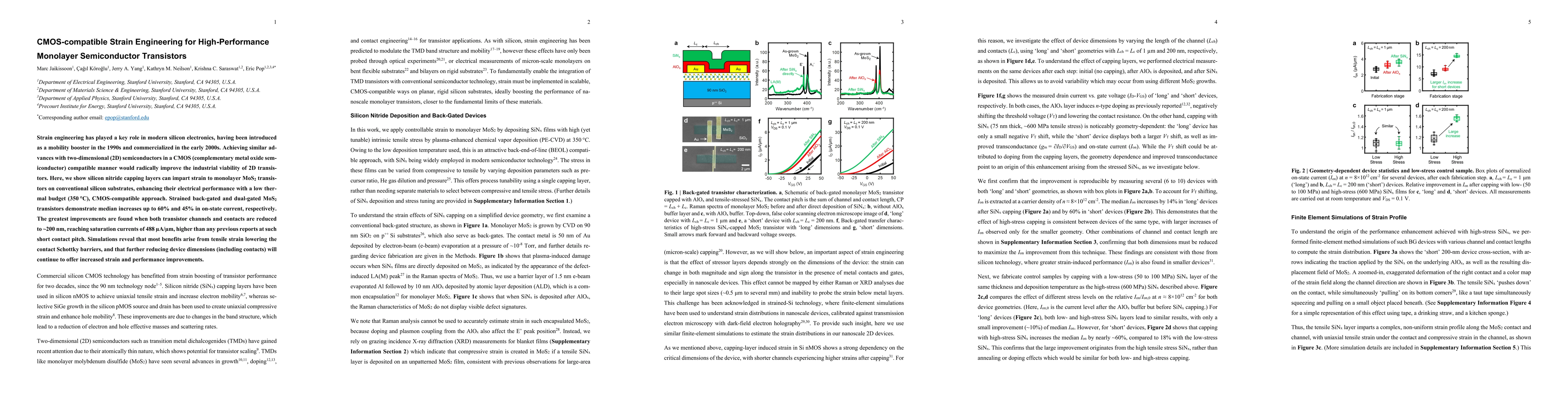
Strain engineering has played a key role in modern silicon electronics, having been introduced as a mobility booster in the 1990s and commercialized in the early 2000s. Achieving similar advances wi...
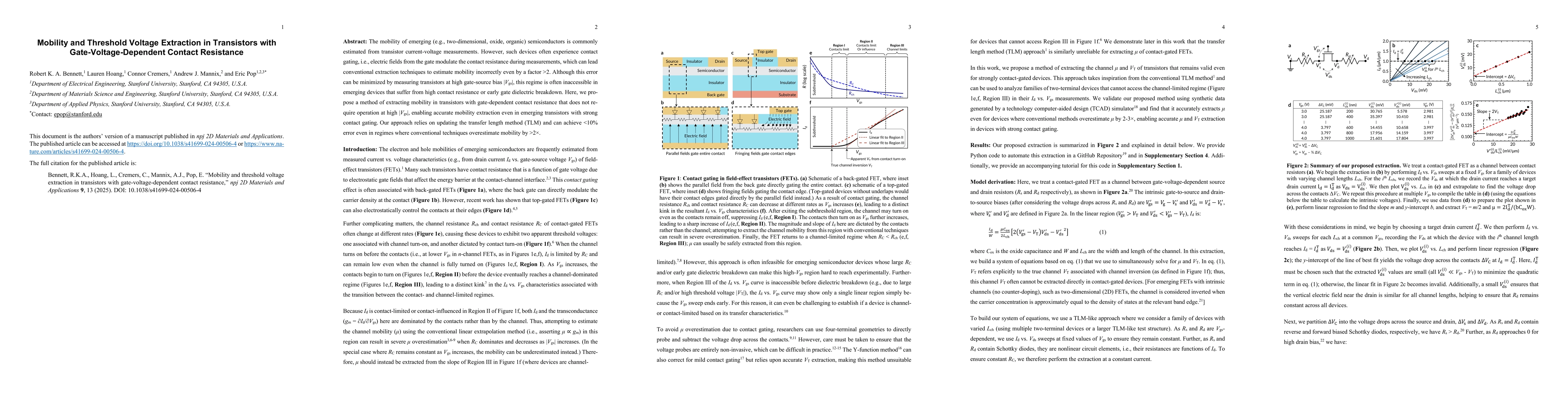
The mobility of emerging (e.g., two-dimensional, oxide, organic) semiconductors is commonly estimated from transistor current-voltage measurements. However, such devices often experience contact gat...
Two-dimensional (2D) semiconducting transition-metal dichalcogenides (TMDCs) are an exciting platform for new excitonic physics and next-generation electronics, creating a strong demand to understan...
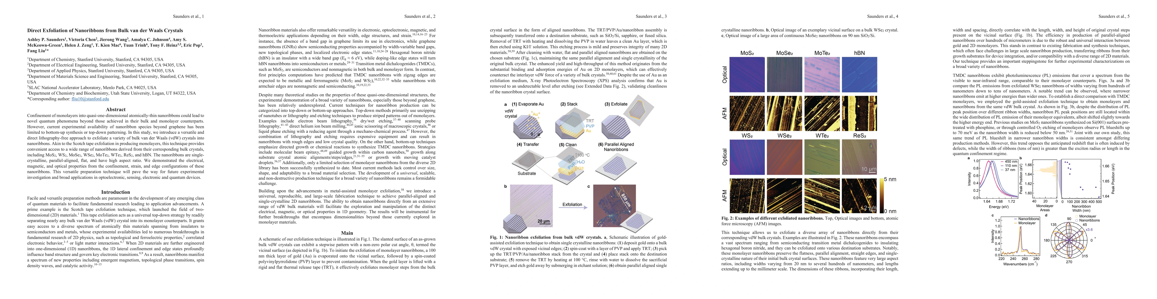
Confinement of monolayers into quasi-one-dimensional atomically-thin nanoribbons could lead to novel quantum phenomena beyond those achieved in their bulk and monolayer counterparts. However, curren...
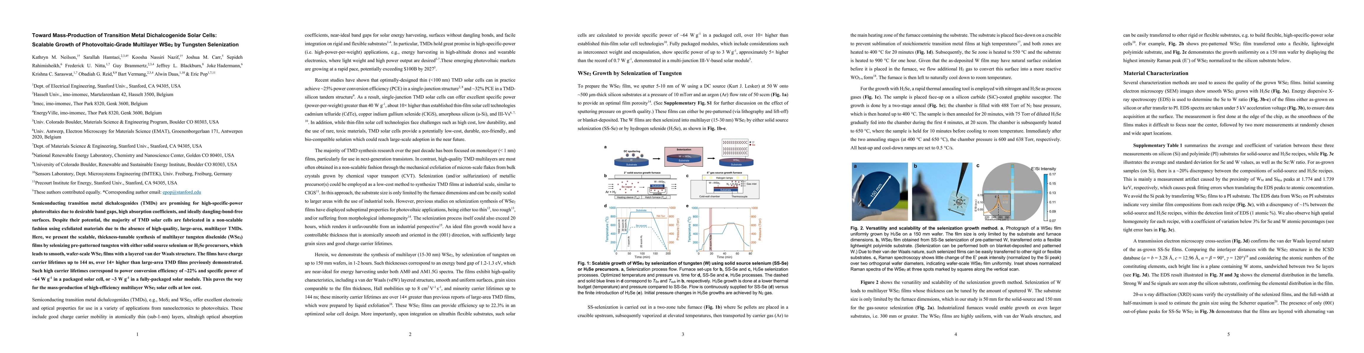
Semiconducting transition metal dichalcogenides (TMDs) are promising for high-specific-power photovoltaics due to desirable band gaps, high absorption coefficients, and ideally dangling-bond-free su...
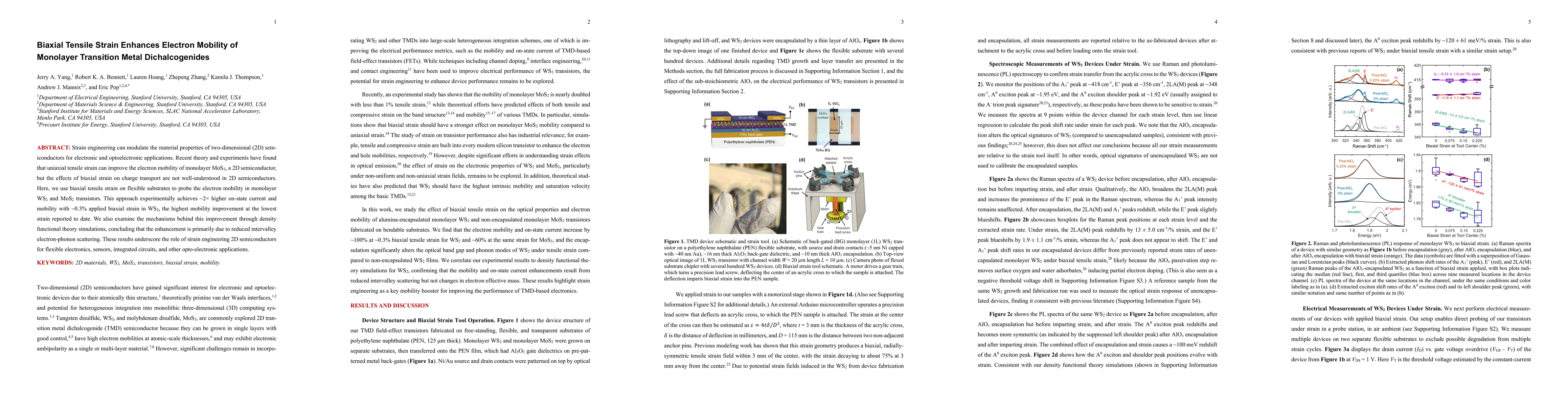
Strain engineering can modulate the material properties of two-dimensional (2D) semiconductors for electronic and optoelectronic applications. Recent theory and experiments have found that uniaxial ...
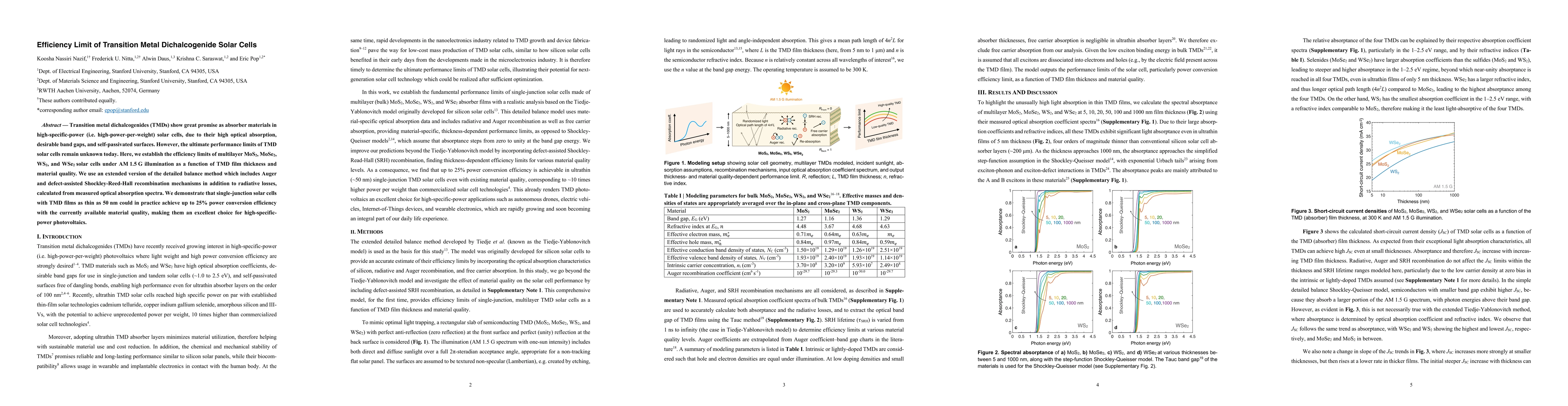
Transition metal dichalcogenides (TMDs) show great promise as absorber materials in high-specific-power (i.e. high-power-per-weight) solar cells, due to their high optical absorption, desirable band...
Free-space modulation of light is crucial for many applications, from light detection and ranging to virtual or augmented reality. Traditional means of modulating free-space light involves spatial l...
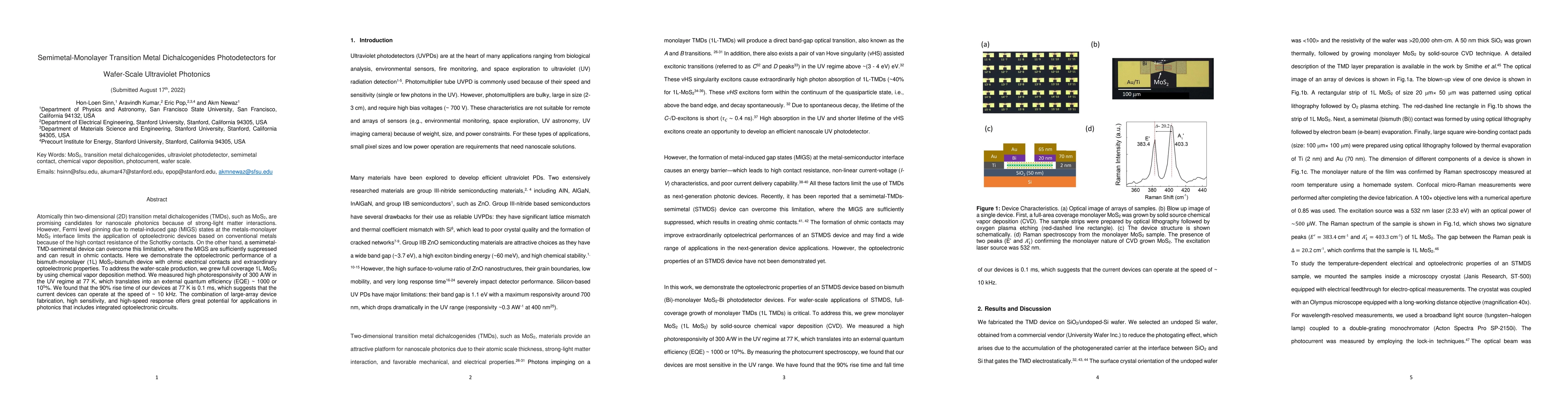
Atomically thin two-dimensional (2D) transition metal dichalcogenides (TMDs), such as MoS$_2$, are promising candidates for nanoscale photonics because of strong-light matter interactions. However, ...
When transistor gate insulators have nanometer-scale equivalent oxide thickness (EOT), the gate capacitance ($C_\textrm{G}$) becomes smaller than the oxide capacitance ($C_\textrm{ox}$) due to the q...
Stateful logic is a digital processing-in-memory technique that could address von Neumann memory bottleneck challenges while maintaining backward compatibility with standard von Neumann architecture...
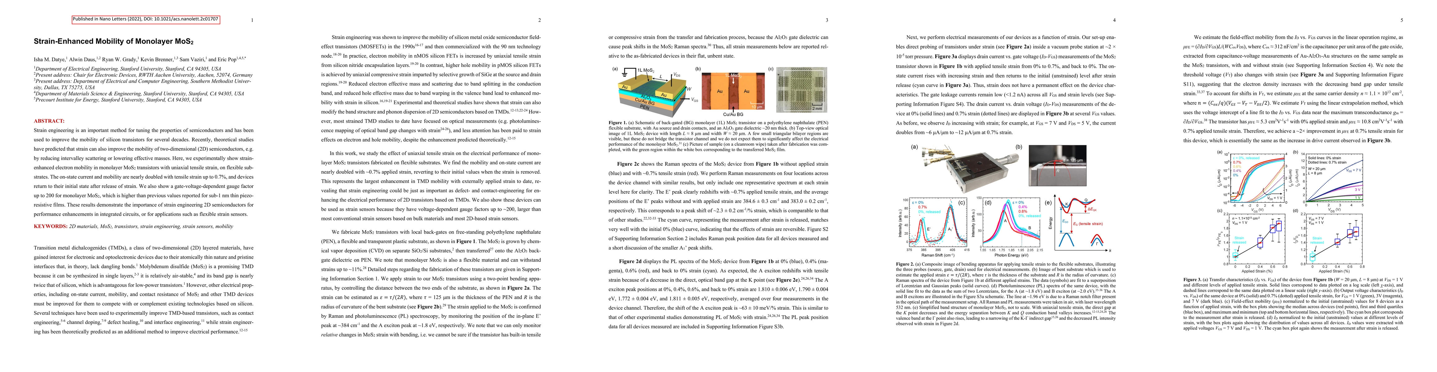
Strain engineering is an important method for tuning the properties of semiconductors and has been used to improve the mobility of silicon transistors for several decades. Recently, theoretical stud...
The thermal properties of two-dimensional (2D) materials, like MoS$_2$, are known to be affected by interactions with their environment, but this has primarily been studied only with SiO$_2$ substra...
Accurate measurements and physical understanding of thermal boundary resistance (R) of two-dimensional (2D) materials are imperative for effective thermal management of 2D electronics and photonics....
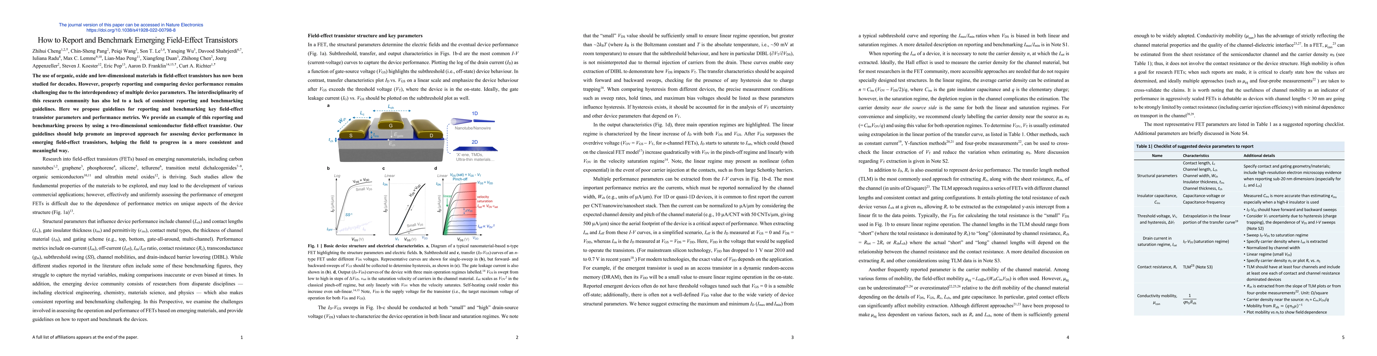
Emerging low-dimensional nanomaterials have been studied for decades in device applications as field-effect transistors (FETs). However, properly reporting and comparing device performance has been ...
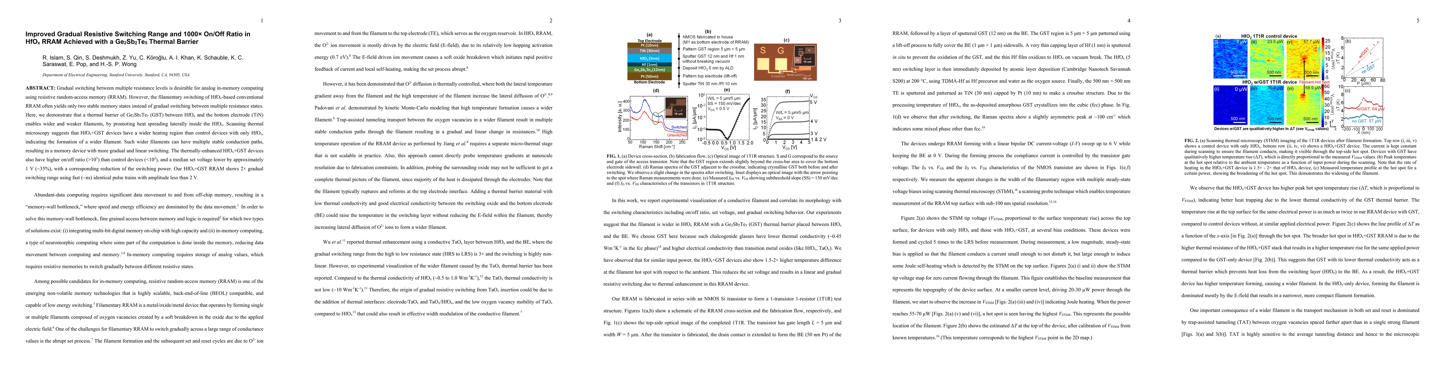
Gradual switching between multiple resistance levels is desirable for analog in-memory computing using resistive random-access memory (RRAM). However, the filamentary switching of $HfO_x$-based conv...
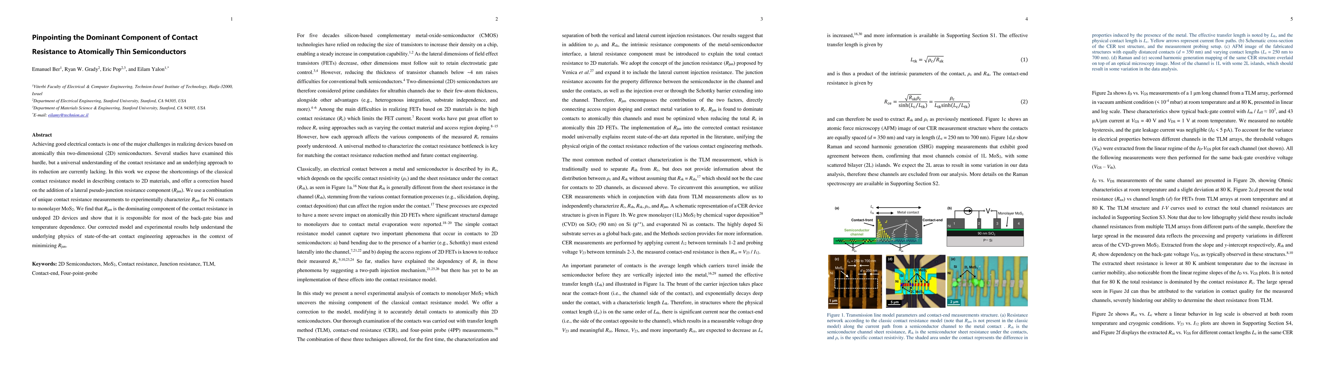
Achieving good electrical contacts is one of the major challenges in realizing devices based on atomically thin two-dimensional (2D) semiconductors. Several studies have examined this hurdle, but a ...
Two-dimensional (2D) semiconductors have been proposed for heterogeneous integration with existing silicon technology; however, their chemical vapor deposition (CVD) growth temperatures are often to...
Structural colors generated due to light scattering from static all-dielectric metasurfaces have successfully enabled high-resolution, high-saturation, and wide-gamut color printing applications. De...
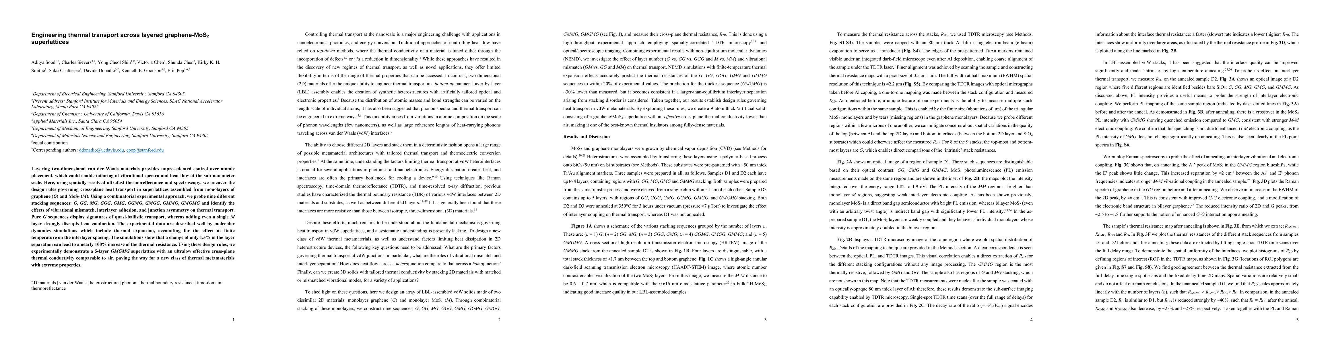
Layering two-dimensional van der Waals materials provides unprecedented control over atomic placement, which could enable tailoring of vibrational spectra and heat flow at the sub-nanometer scale. H...
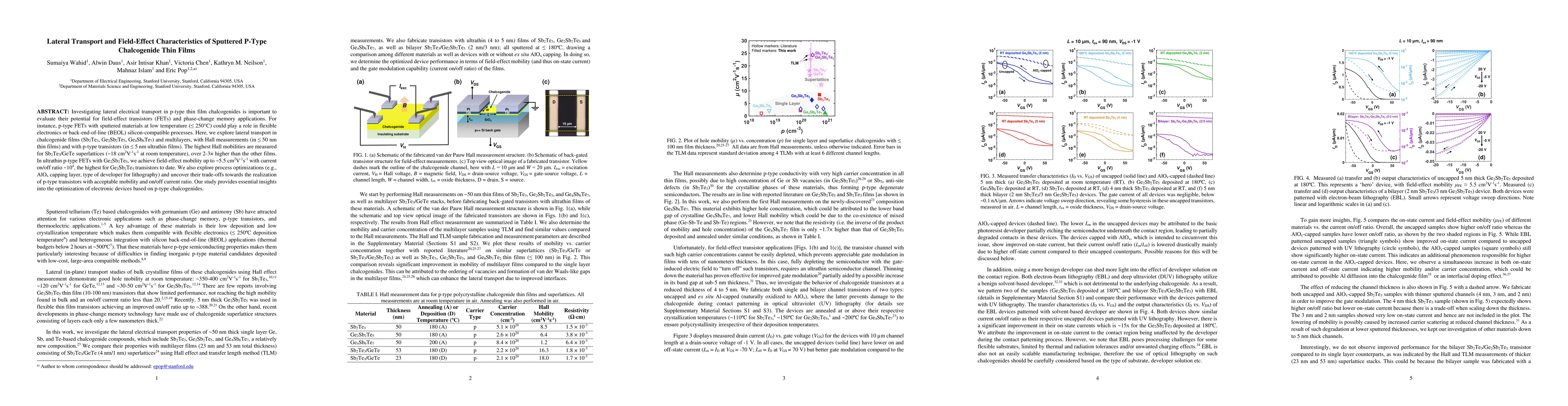
Investigating lateral electrical transport in p-type thin film chalcogenides is important to evaluate their potential for field-effect transistors (FETs) and phase-change memory applications. For in...
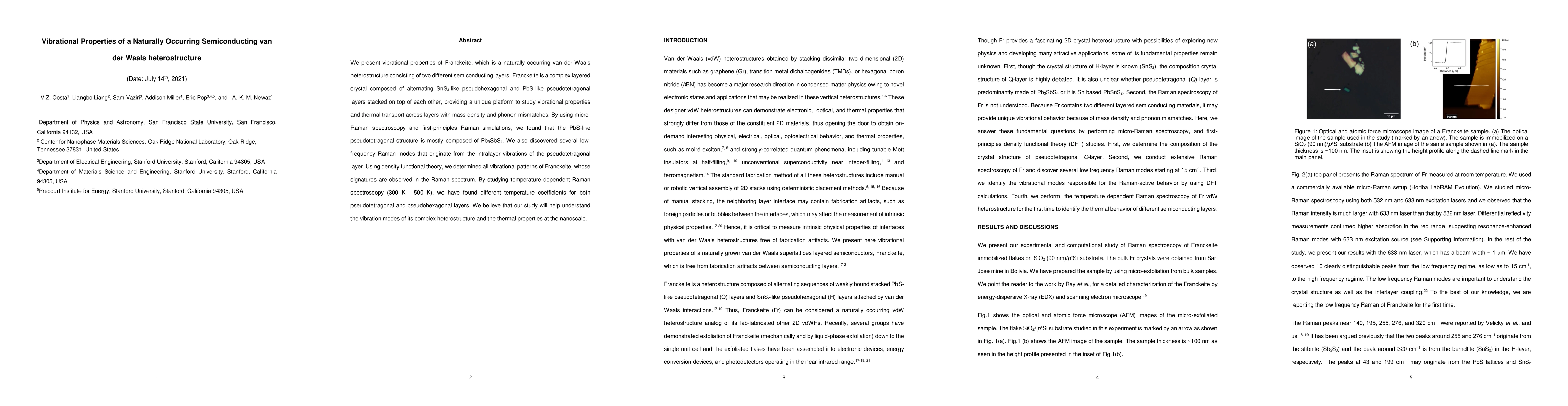
We present vibrational properties of Franckeite, which is a naturally occurring van der Waals heterostructure consisting of two different semiconducting layers. Franckeite is a complex layered cryst...
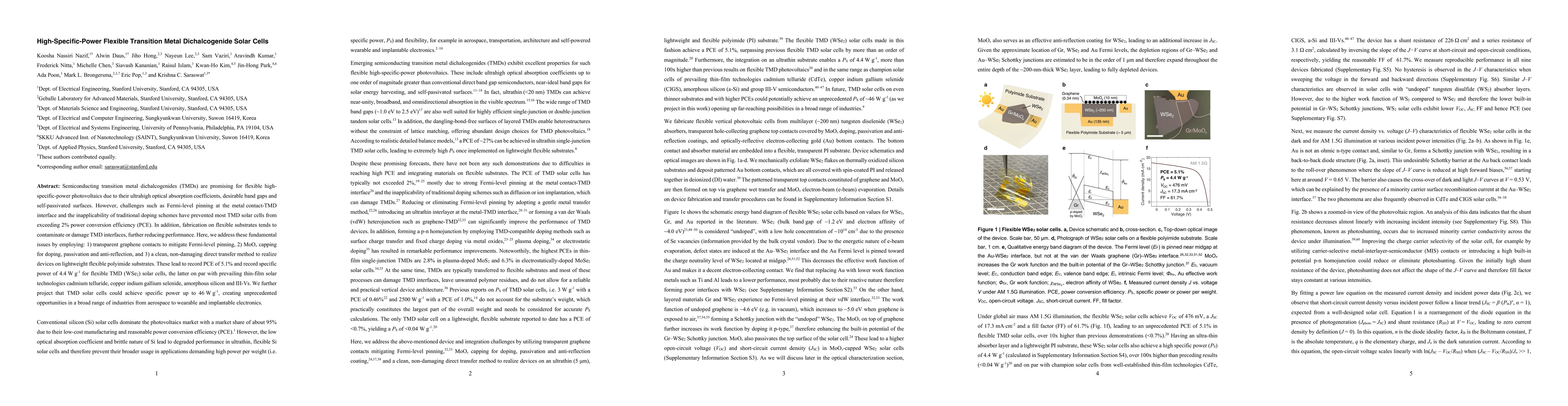
Semiconducting transition metal dichalcogenides (TMDs) are promising for flexible high-specific-power photovoltaics due to their ultrahigh optical absorption coefficients, desirable band gaps and se...
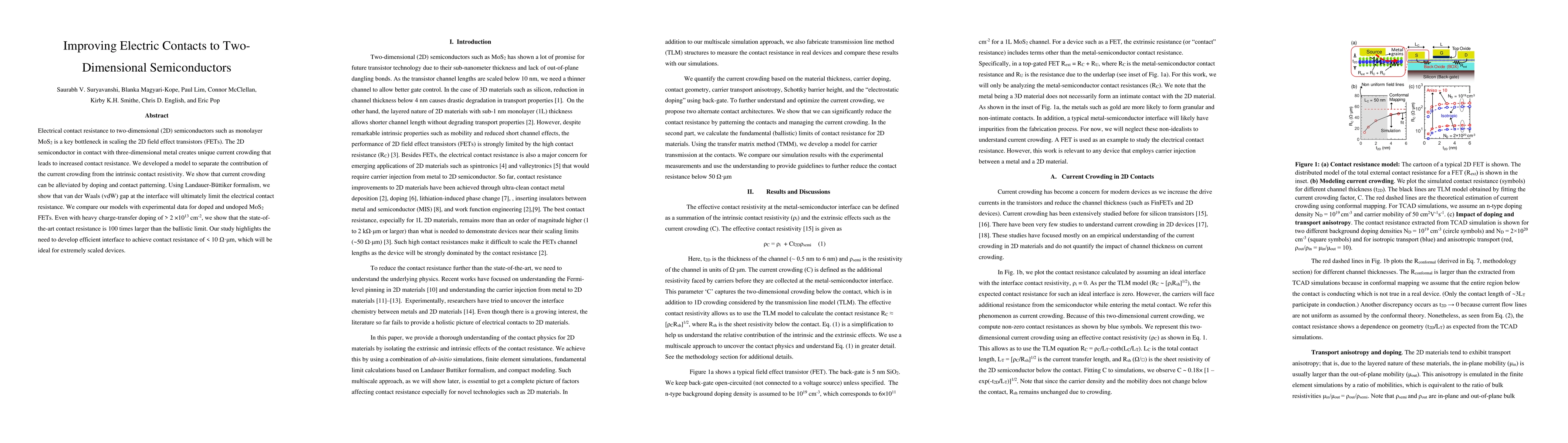
Electrical contact resistance to two-dimensional (2D) semiconductors such as monolayer MoS_{2} is a key bottleneck in scaling the 2D field effect transistors (FETs). The 2D semiconductor in contact ...
We present a scaling theory of two-dimensional (2D) field effect transistors (FETs). For devices with channel thickness less than 4 nm, the device electrostatics is dominated by the physical gate ox...
Despite recent advances in active metaoptics, wide dynamic range combined with high-speed reconfigurable solutions is still elusive. Phase-change materials (PCMs) offer a compelling platform for met...
The design of new applications, especially those based on heterogeneous integration, must rely on detailed knowledge of material properties, such as thermal conductivity (TC). To this end, multiple ...
The inferior electrical contact to two-dimensional (2D) materials is a critical challenge for their application in post-silicon very large-scale integrated circuits. Electrical contacts were general...
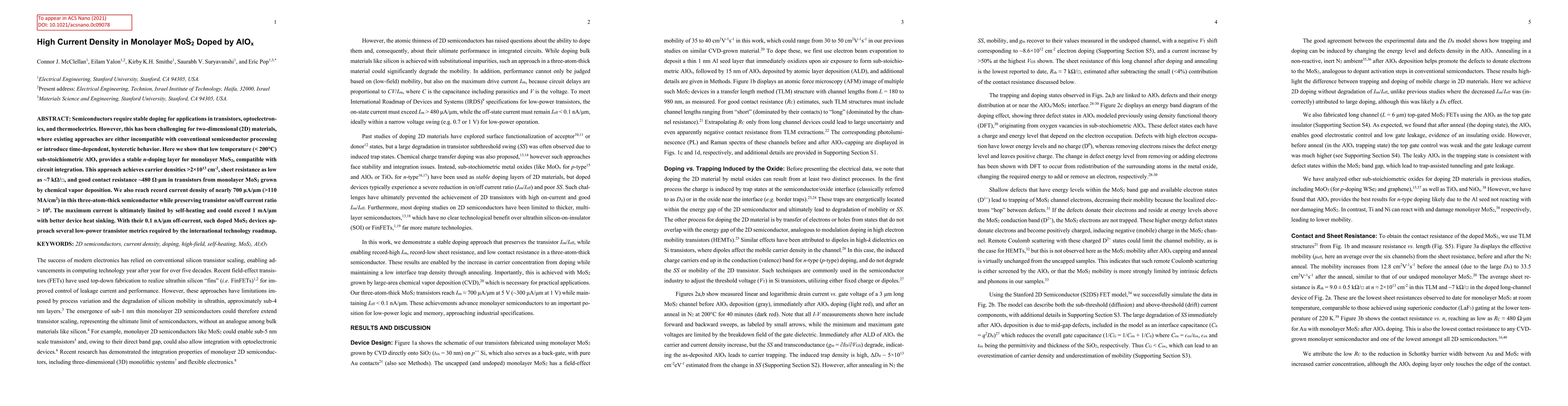
Semiconductors require stable doping for applications in transistors, optoelectronics, and thermoelectrics. However, this has been challenging for two-dimensional (2D) materials, where existing appr...
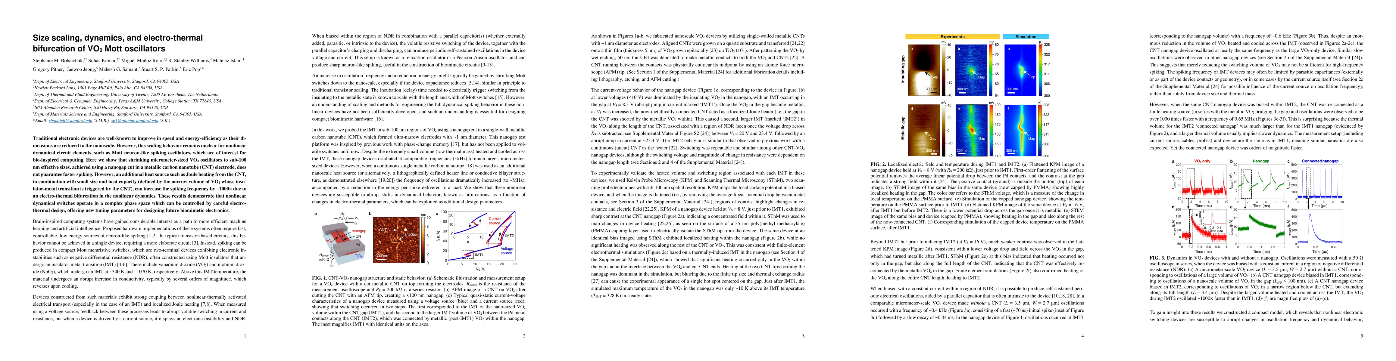
Traditional electronic devices are well-known to improve in speed and energy-efficiency as their dimensions are reduced to the nanoscale. However, this scaling behavior remains unclear for nonlinear...
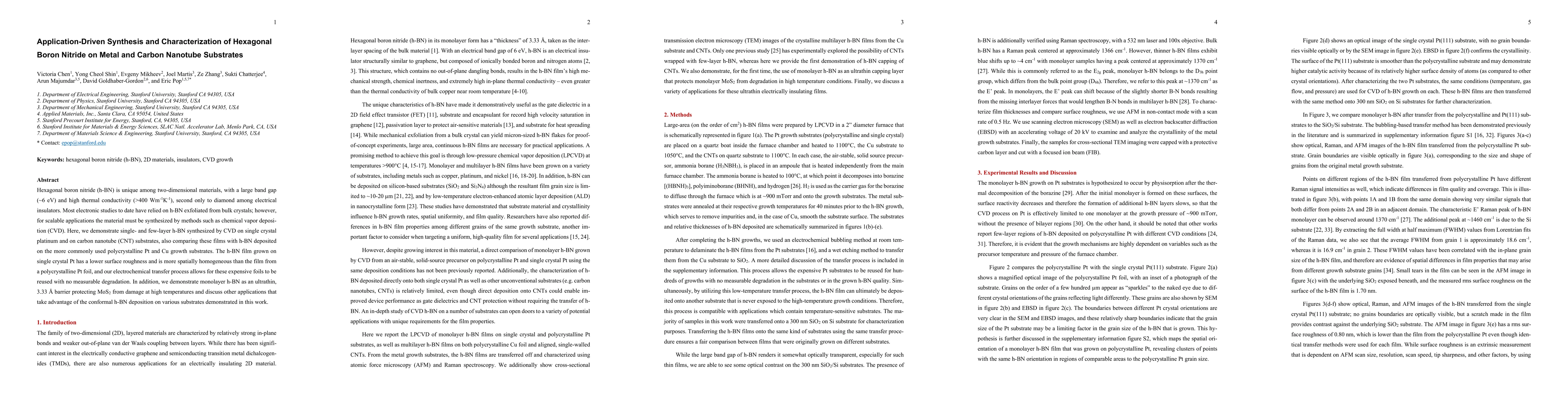
Hexagonal boron nitride (h-BN) is unique among two-dimensional materials, with a large band gap (~6 eV) and high thermal conductivity (>400 W/m/K), second only to diamond among electrical insulators...
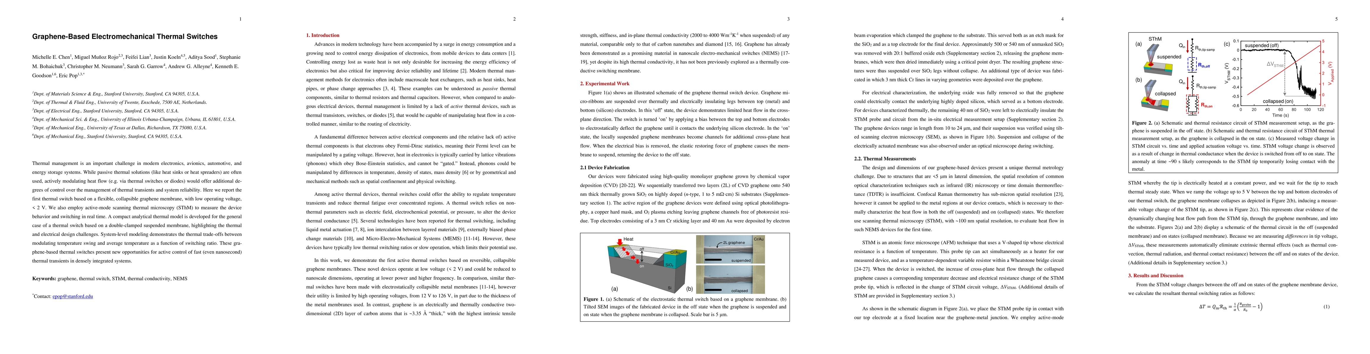
Thermal management is an important challenge in modern electronics, avionics, automotive, and energy storage systems. While passive thermal solutions (like heat sinks or heat spreaders) are often us...
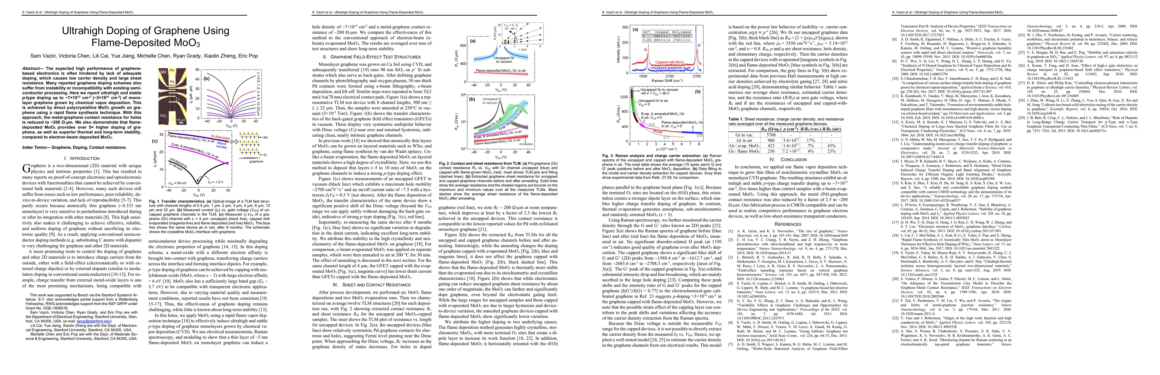
The expected high performance of graphene-based electronics is often hindered by lack of adequate doping, which causes low carrier density and large sheet resistance. Many reported graphene doping s...
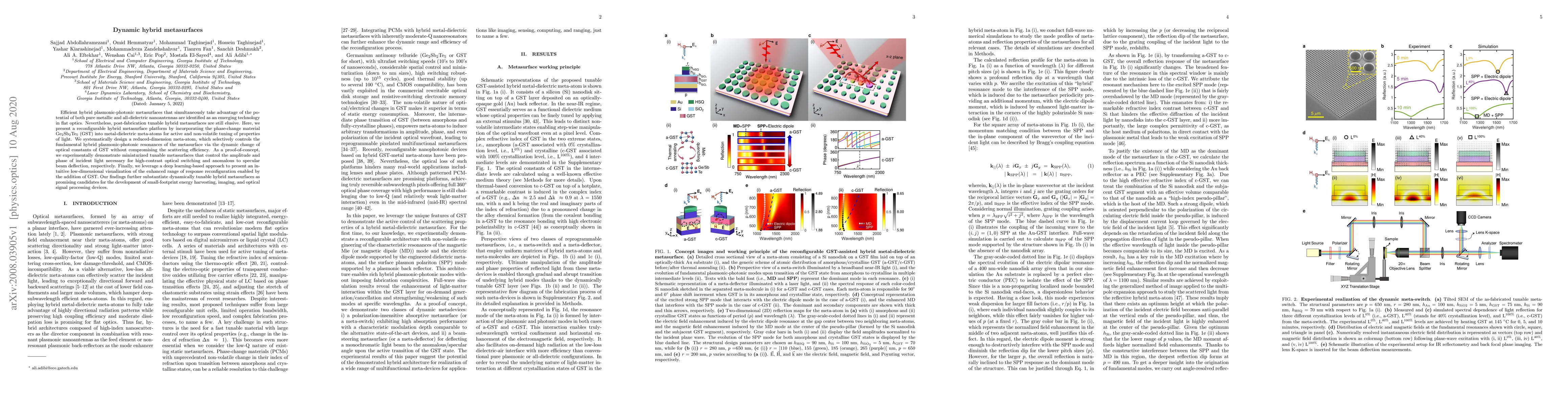
Efficient hybrid plasmonic-photonic metasurfaces that simultaneously take advantage of the potential of both pure metallic and all-dielectric nanoantennas are identified as an emerging technology in...
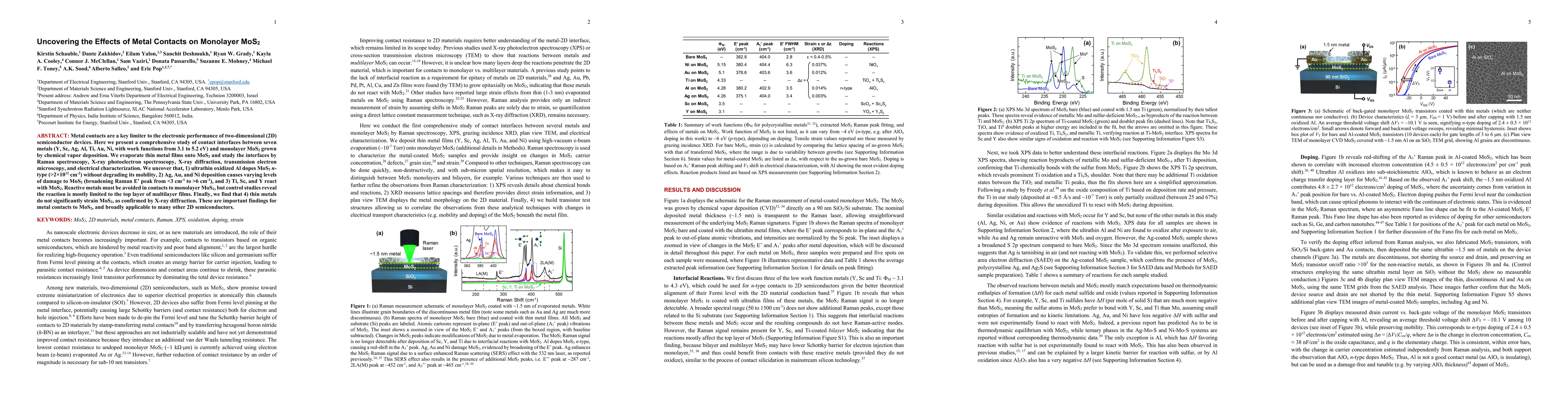
Metal contacts are a key limiter to the electronic performance of two-dimensional (2D) semiconductor devices. Here we present a comprehensive study of contact interfaces between seven metals (Y, Sc,...
Electrical and thermal properties of atomically thin two-dimensional (2D) materials are affected by their environment, e.g. through remote phonon scattering or dielectric screening. However, while i...
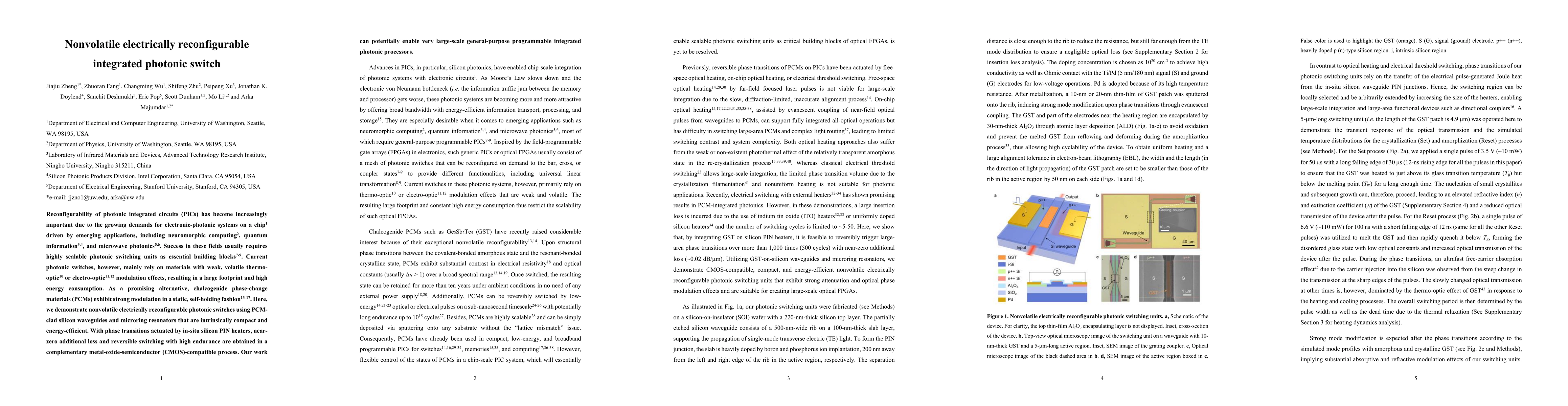
Reconfigurability of photonic integrated circuits (PICs) has become increasingly important due to the growing demands for electronic-photonic systems on a chip driven by emerging applications, inclu...
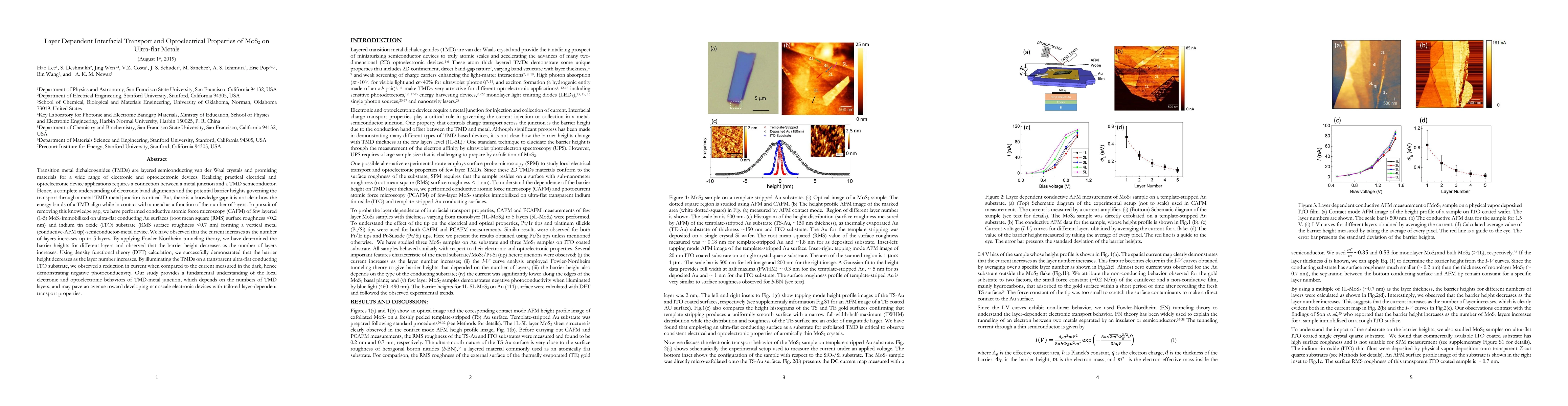
Transition metal dichalcogenides (TMDs) are layered semiconducting van der Waal crystals and promising materials for a wide range of electronic and optoelectronic devices. Realizing practical electr...
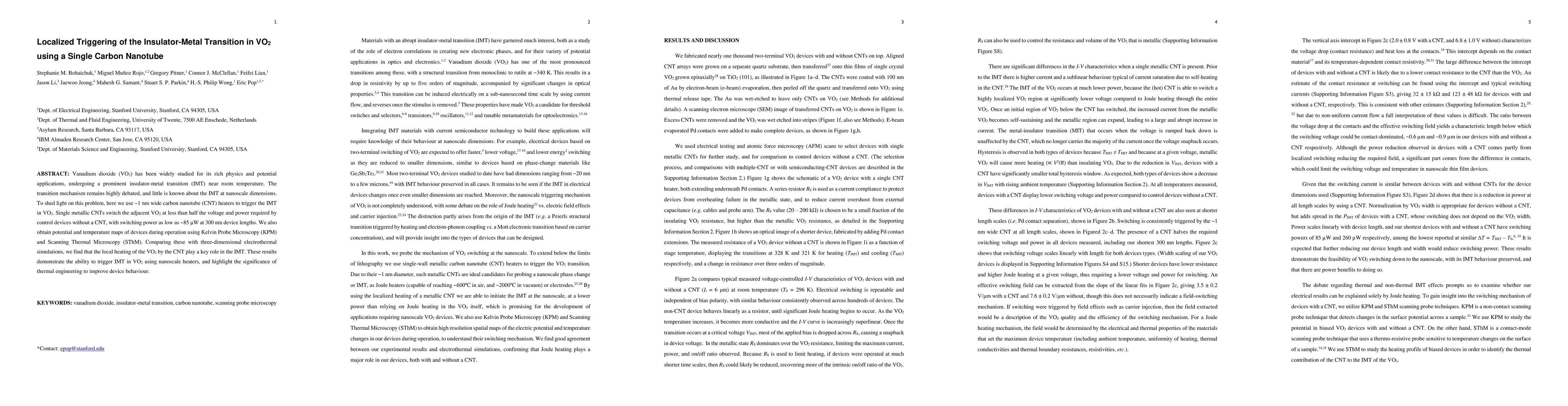
Vanadium dioxide (VO2) has been widely studied for its rich physics and potential applications, undergoing a prominent insulator-metal transition (IMT) near room temperature. The transition mechanis...
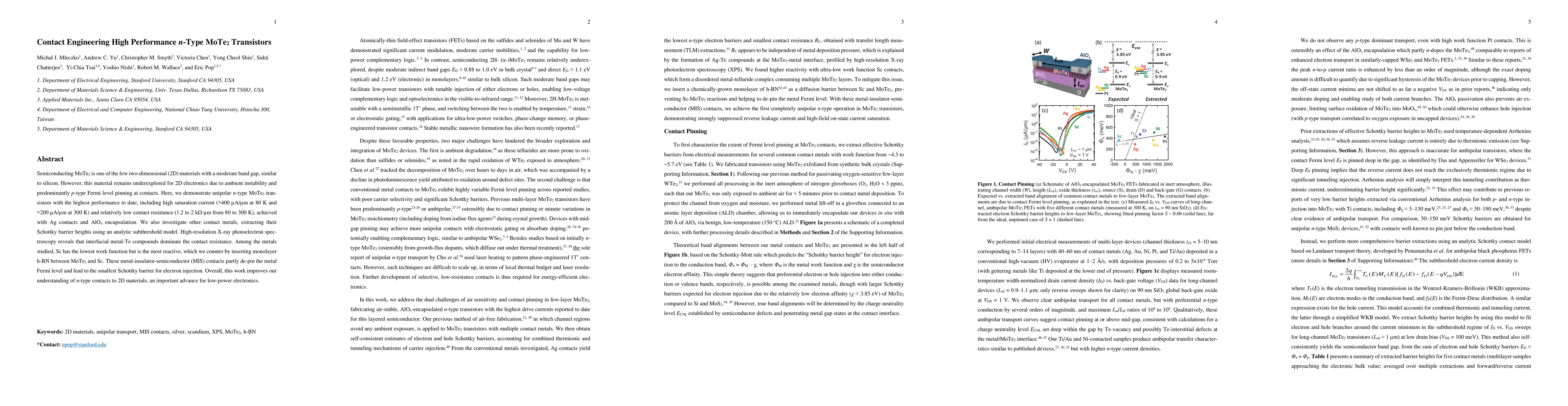
Semiconducting MoTe2 is one of the few two-dimensional (2D) materials with a moderate band gap, similar to silicon. However, this material remains under-explored for 2D electronics due to ambient in...
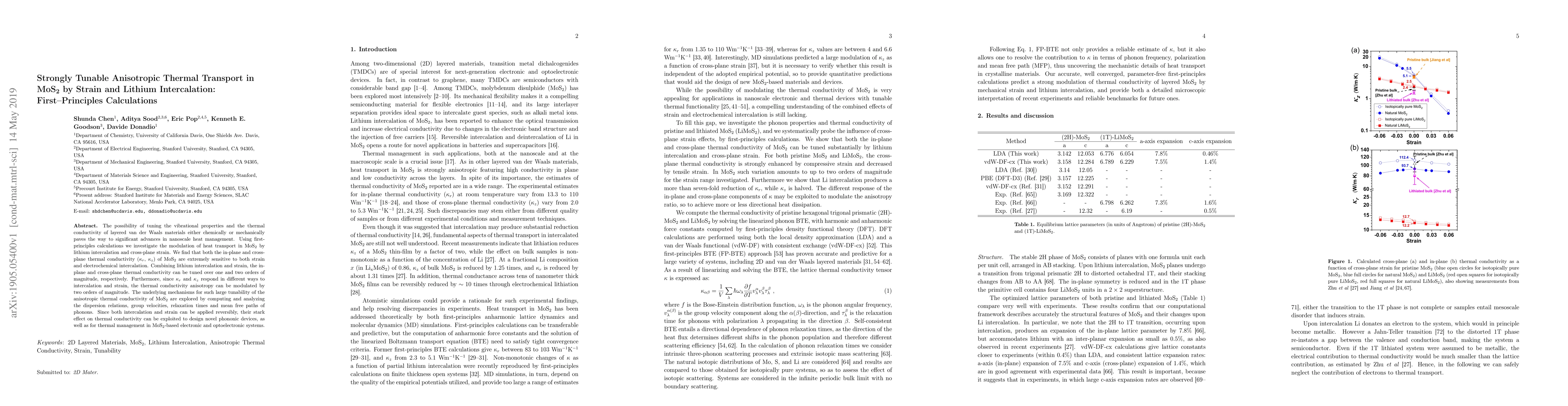
The possibility of tuning the vibrational properties and the thermal conductivity of layered van der Waals materials either chemically or mechanically paves the way to significant advances in nanosc...
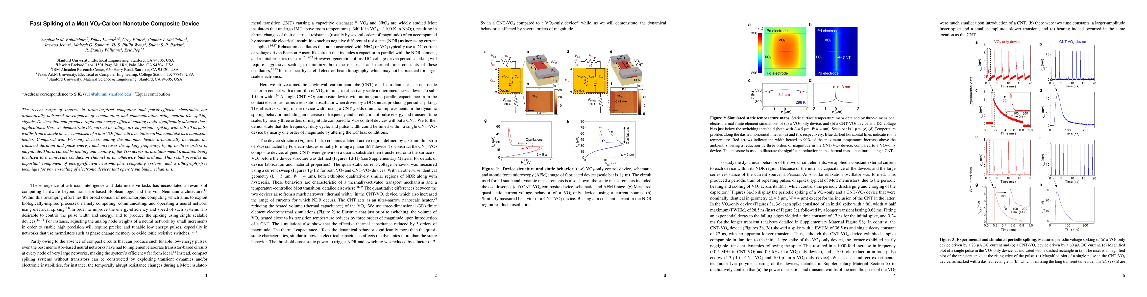
The recent surge of interest in brain-inspired computing and power-efficient electronics has dramatically bolstered development of computation and communication using neuron-like spiking signals. De...
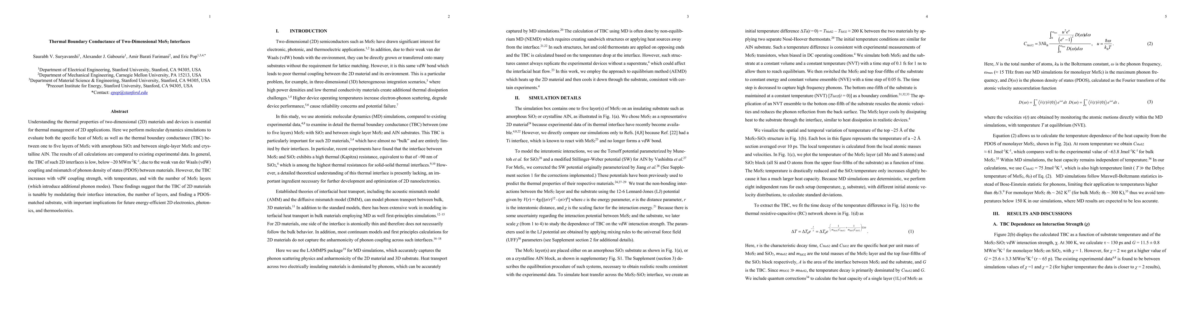
Understanding the thermal properties of two-dimensional (2D) materials and devices is essential for thermal management of 2D applications. Here we perform molecular dynamics simulations to evaluate ...
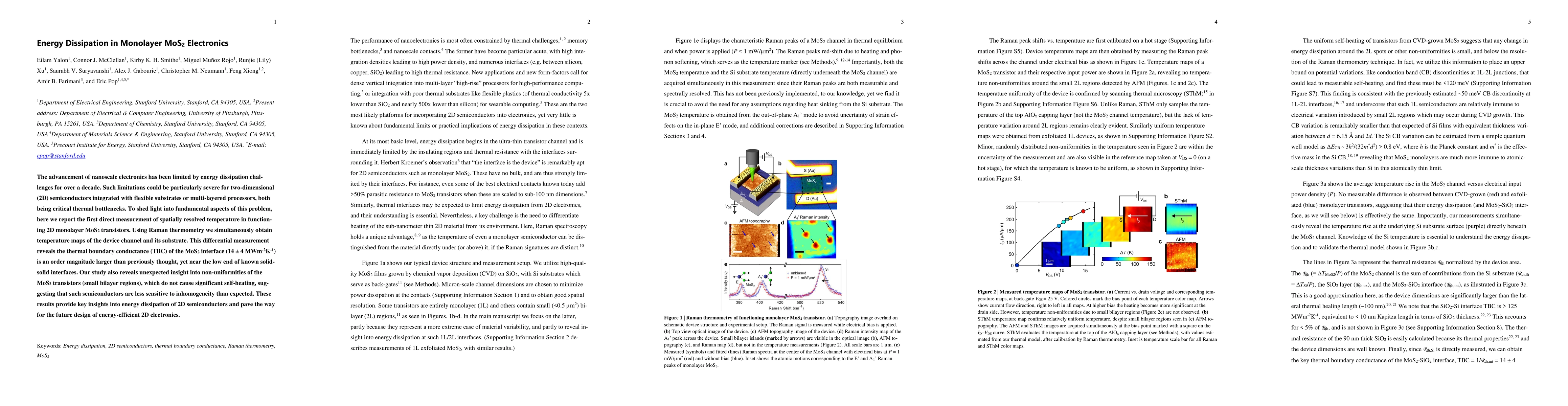
The advancement of nanoscale electronics has been limited by energy dissipation challenges for over a decade. Such limitations could be particularly severe for two-dimensional (2D) semiconductors in...
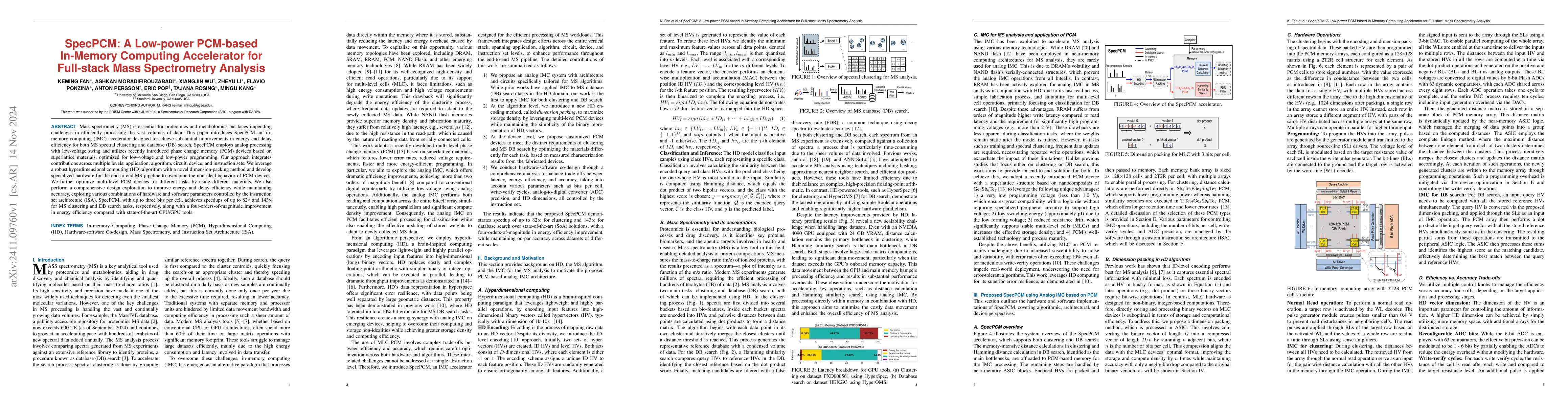
Mass spectrometry (MS) is essential for proteomics and metabolomics but faces impending challenges in efficiently processing the vast volumes of data. This paper introduces SpecPCM, an in-memory compu...
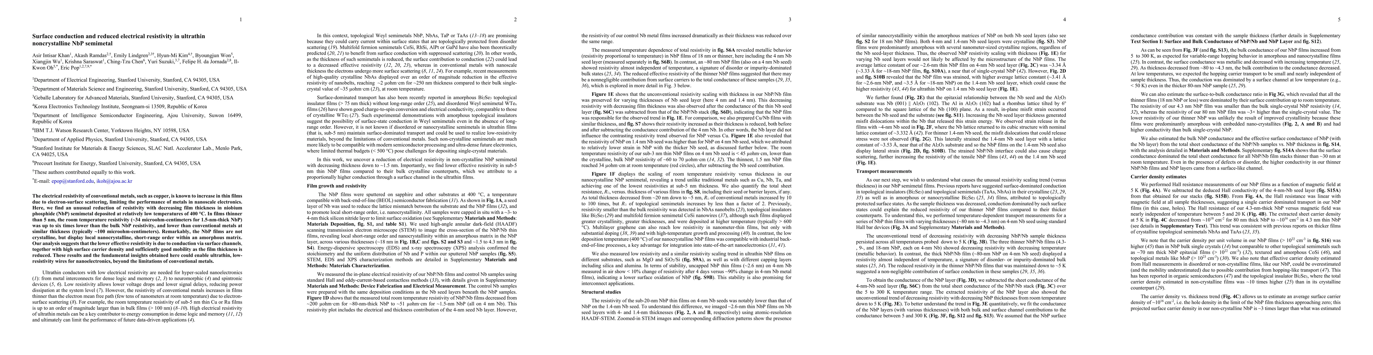
The electrical resistivity of conventional metals, such as copper, is known to increase in thinner films due to electron-surface scattering, limiting the performance of metals in nanoscale electronics...
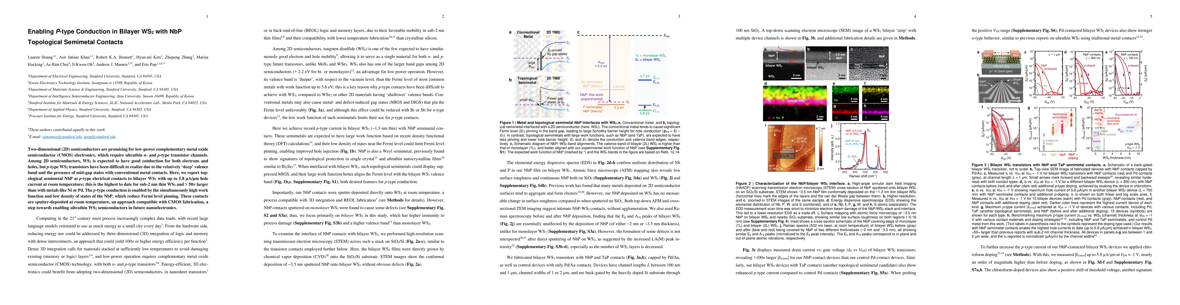
Two-dimensional (2D) semiconductors are promising for low-power complementary metal oxide semiconductor (CMOS) electronics, which require ultrathin n- and p-type transistor channels. Among 2D semicond...
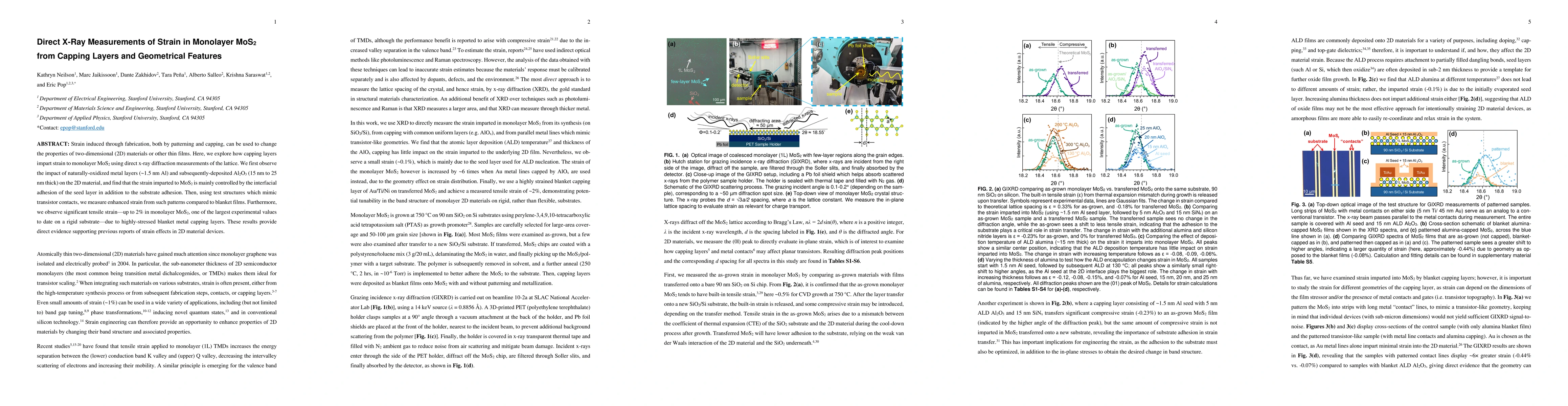
Strain induced through fabrication, both by patterning and capping, can be used to change the properties of two-dimensional (2D) materials or other thin films. Here, we explore how capping layers impa...
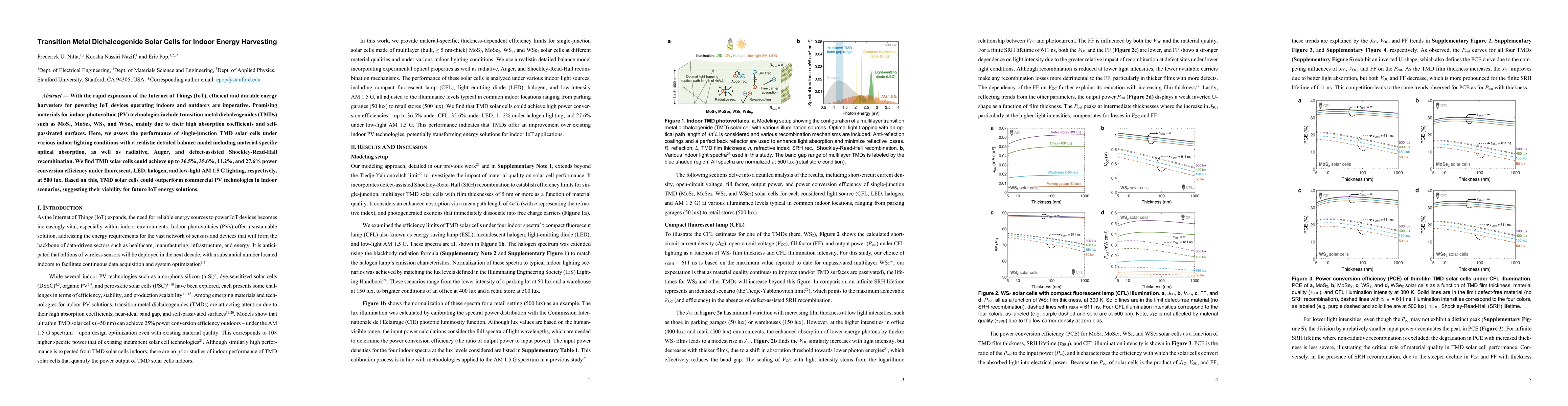
With the rapid expansion of the Internet of Things (IoT), efficient and durable energy harvesters for powering IoT devices operating indoors and outdoors are imperative. Promising materials for indoor...
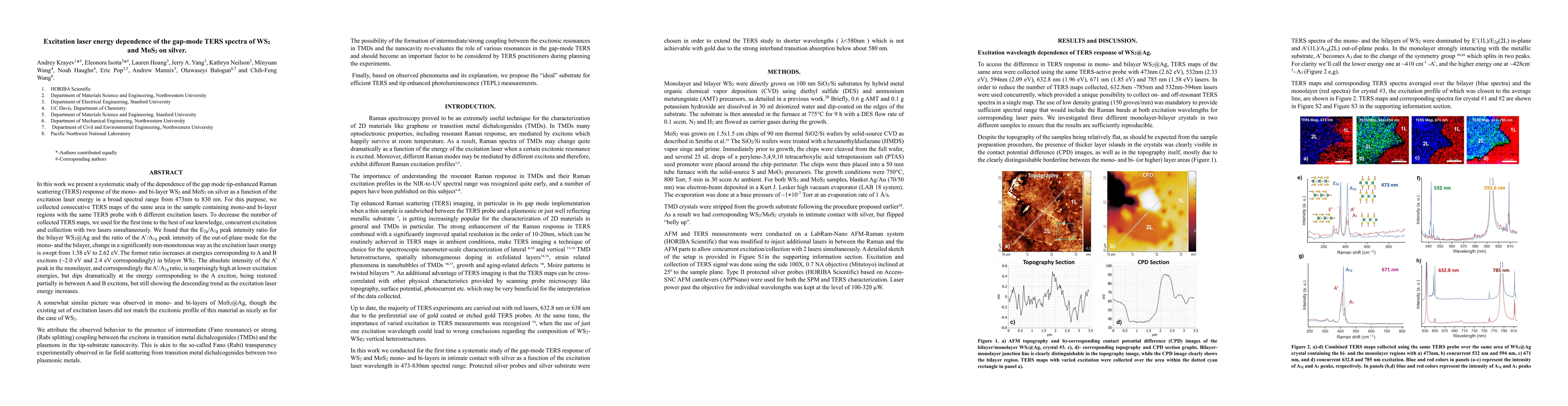
We present a systematic study of the dependence of gap mode tip-enhanced Raman scattering (TERS) of mono- and bi-layer WS$_2$ and MoS$_2$ as a function of excitation laser energy. We collected consecu...
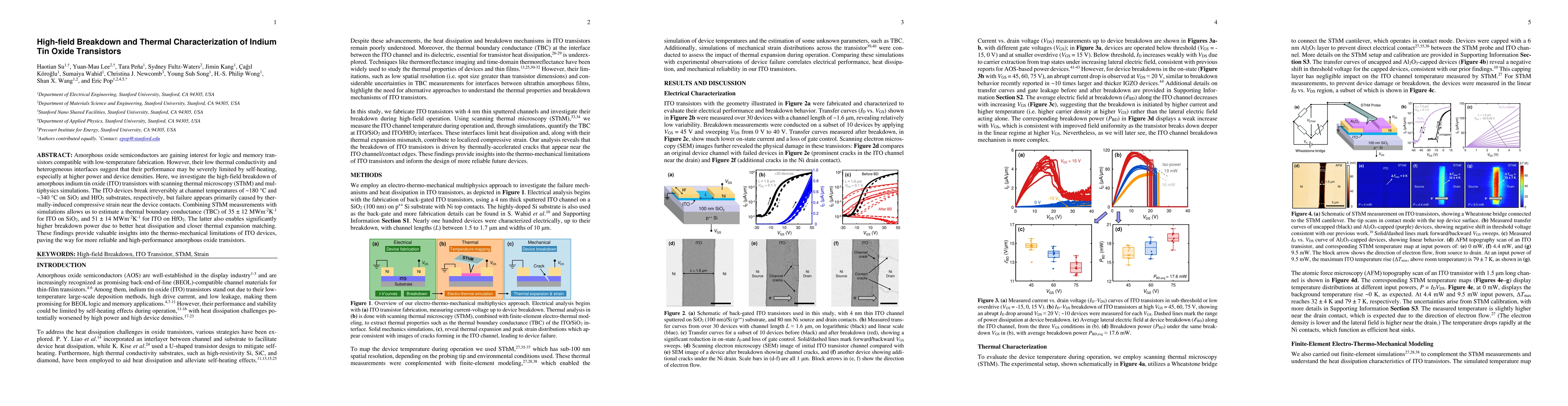
Amorphous oxide semiconductors are gaining interest for logic and memory transistors compatible with low-temperature fabrication. However, their low thermal conductivity and heterogeneous interfaces s...
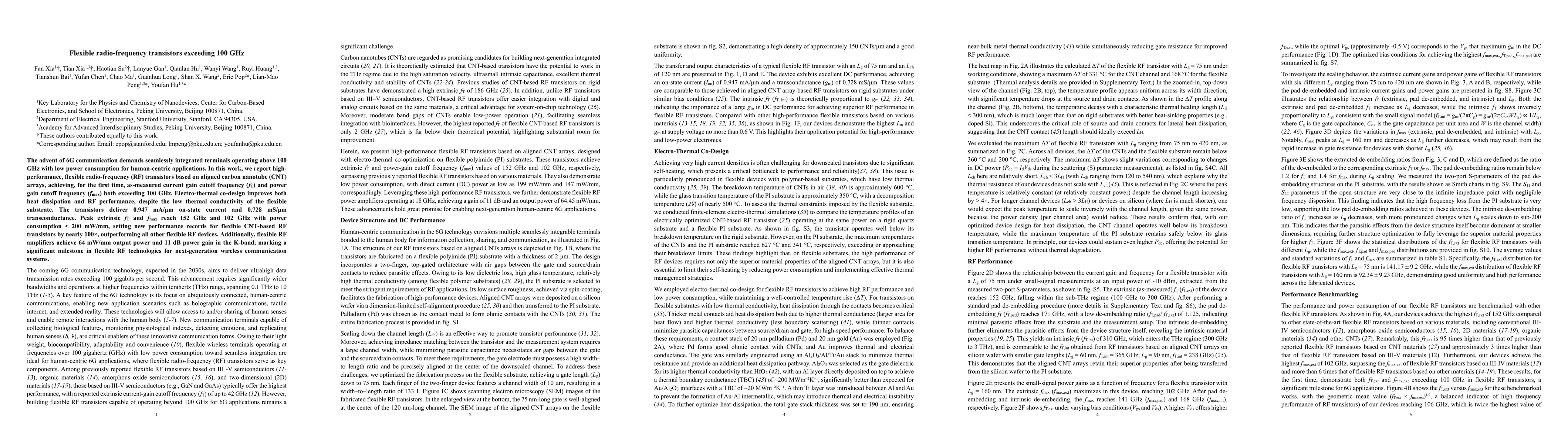
The advent of 6G communication demands seamlessly integrated terminals operating above 100 GHz with low power consumption for human-centric applications. In this work, we report high-performance, flex...
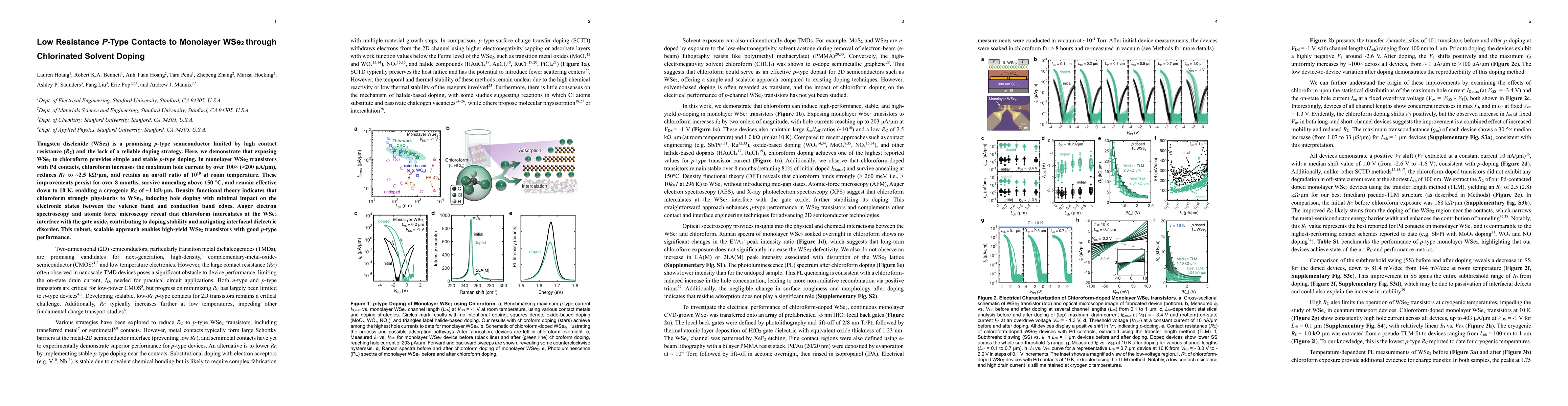
Tungsten diselenide (WSe$_2$) is a promising p-type semiconductor limited by high contact resistance ($R_\textrm{C}$) and the lack of a reliable doping strategy. Here, we demonstrate that exposing WSe...
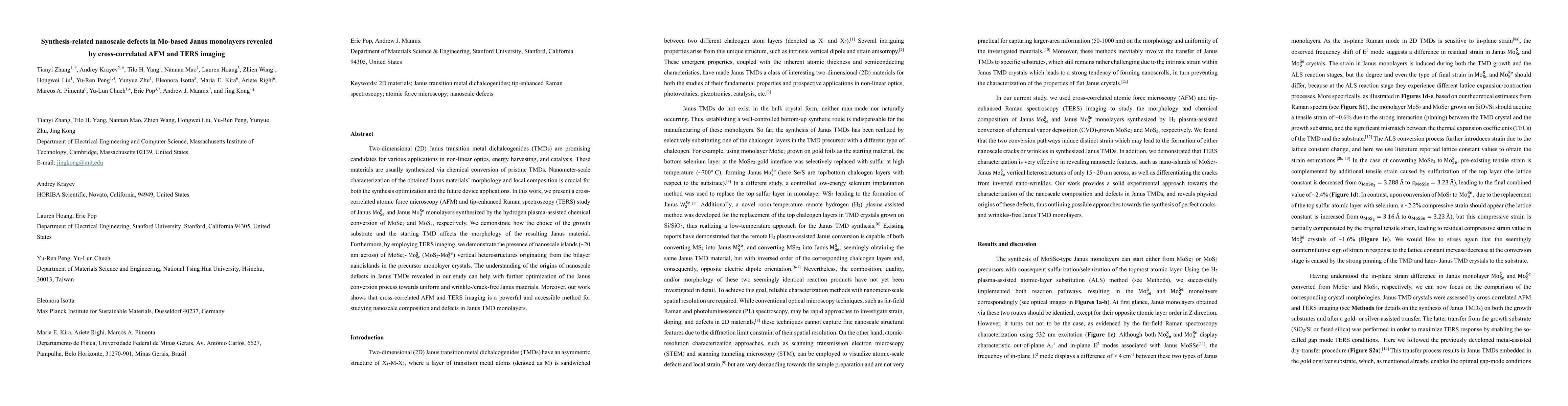
Two-dimensional (2D) Janus transition metal dichalcogenides (TMDs) are promising candidates for various applications in non-linear optics, energy harvesting, and catalysis. These materials are usually...
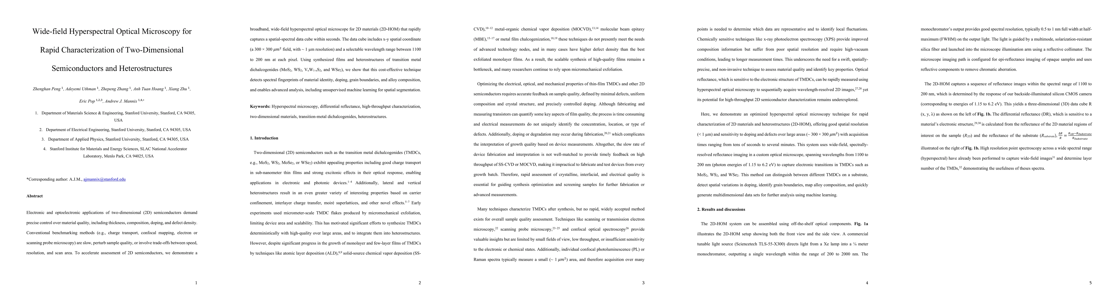
Electronic and optoelectronic applications of two-dimensional (2D) semiconductors demand precise control over material quality, including thickness, composition, doping, and defect density. Convention...
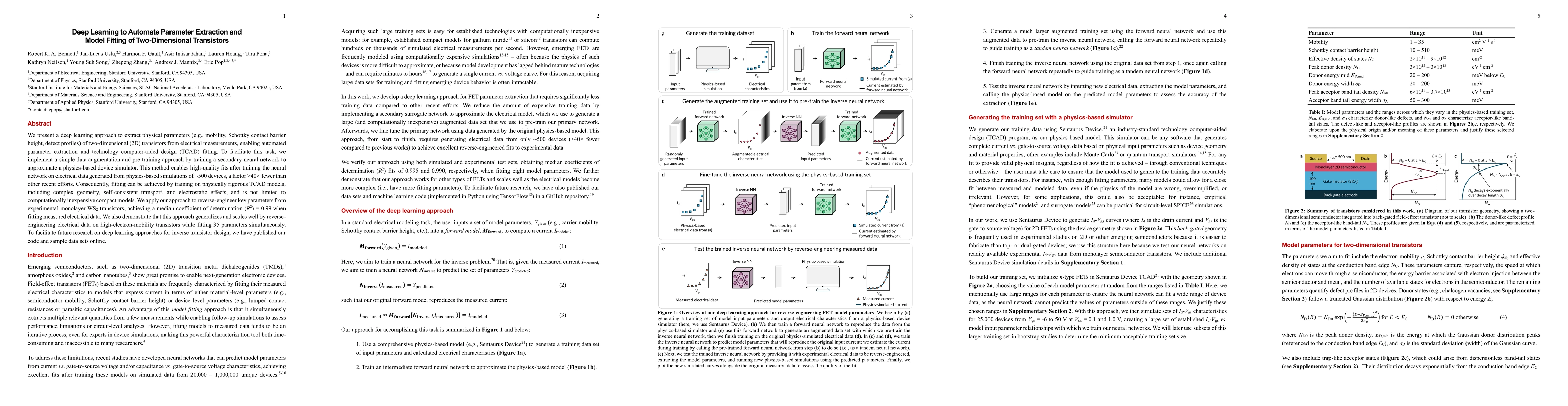
We present a deep learning approach to extract physical parameters (e.g., mobility, Schottky contact barrier height, defect profiles) of two-dimensional (2D) transistors from electrical measurements, ...
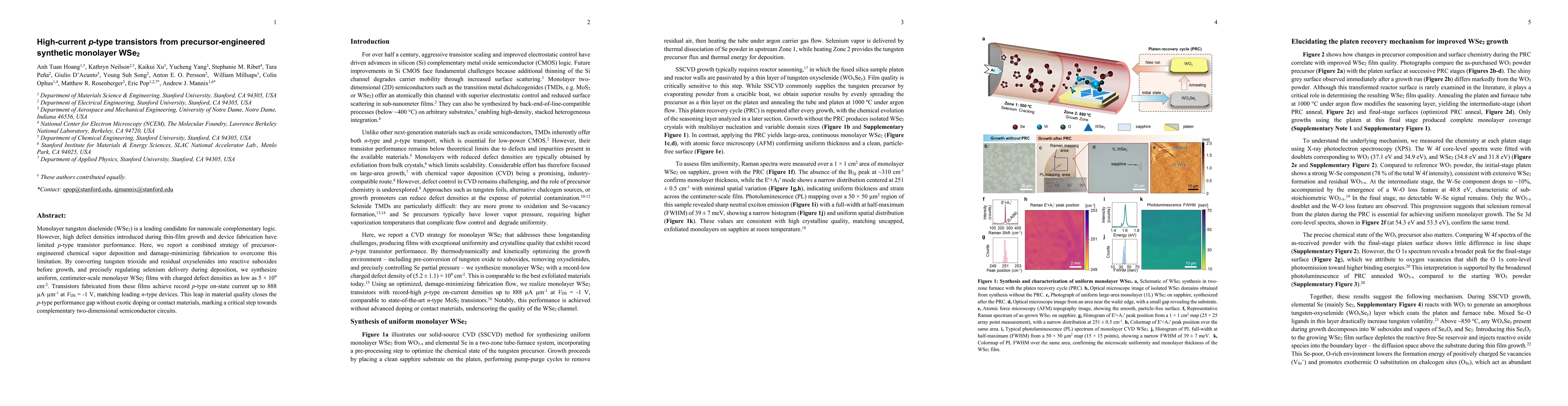
Monolayer tungsten diselenide (WSe$_2$) is a leading candidate for nanoscale complementary logic. However, high defect densities introduced during thin-film growth and device fabrication have limited ...
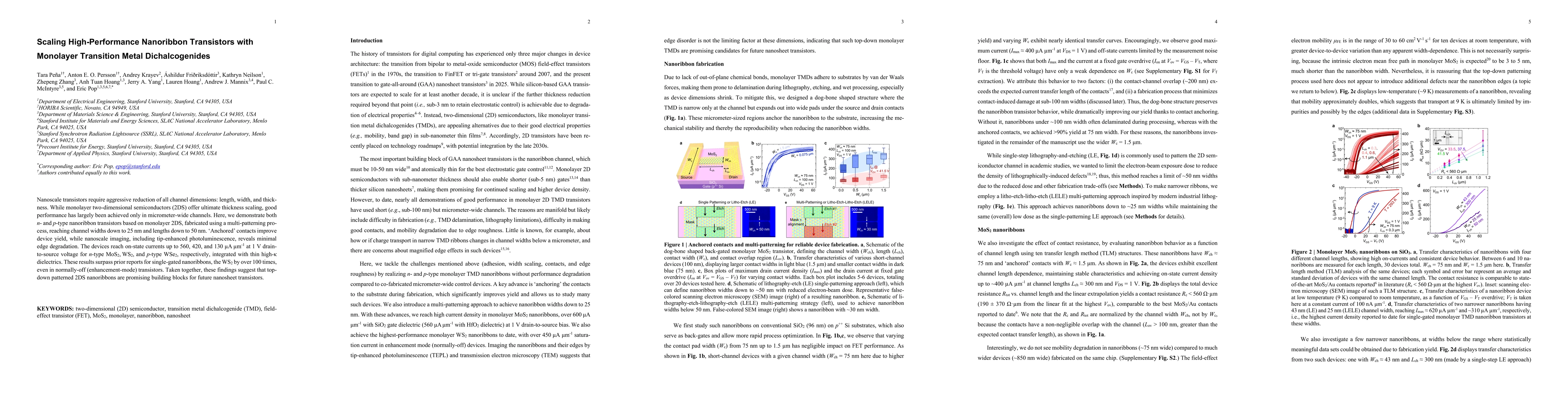
Nanoscale transistors require aggressive reduction of all channel dimensions: length, width, and thickness. While monolayer two-dimensional semiconductors (2DS) offer ultimate thickness scaling, good ...
The recent progress in nanosheet transistors has established two-dimensional (2D) semiconductors as viable candidates for future ultra-scaled electronic devices. Next to reducing contact resistance, i...
We demonstrate a gate dielectric engineering approach leveraging an ultrathin, atomic layer deposited (ALD) silicon oxide interfacial layer (SiL) between the amorphous oxide semiconductor (AOS) channe...
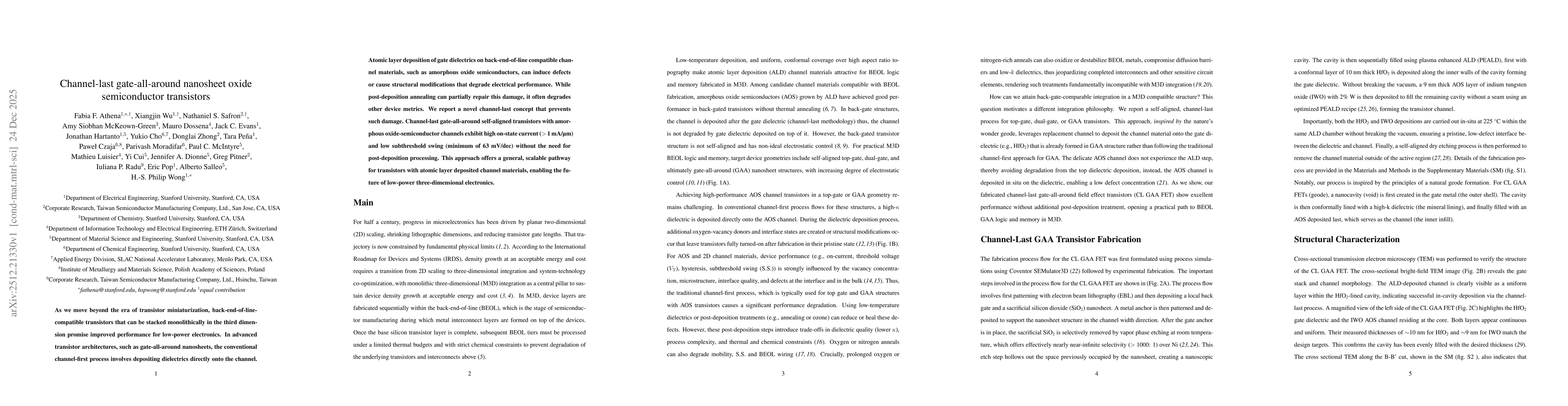
As we move beyond the era of transistor miniaturization, back-end-of-line-compatible transistors that can be stacked monolithically in the third dimension promise improved performance for low-power el...
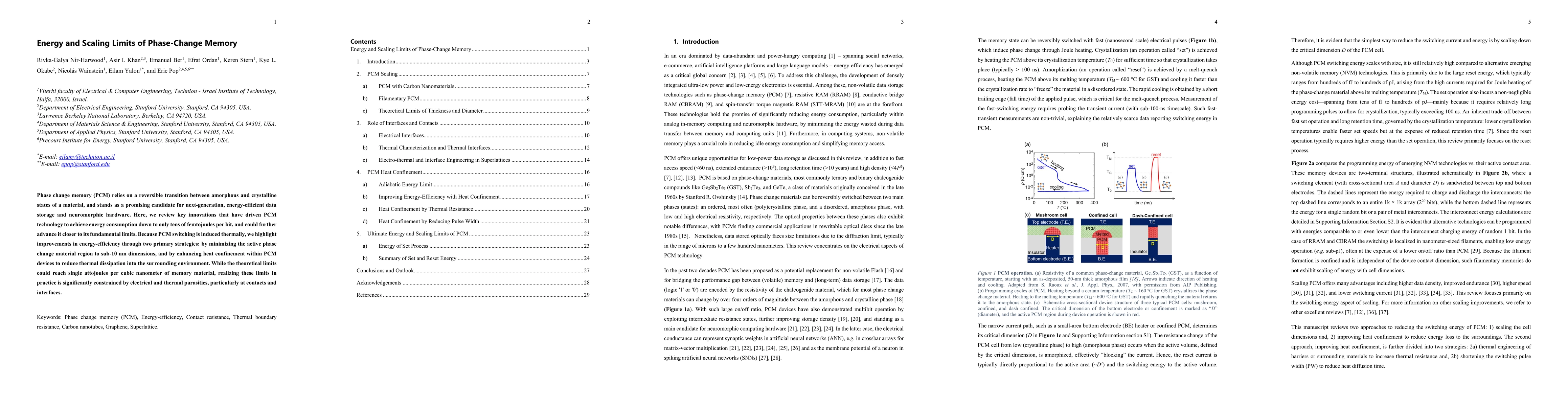
Phase change memory (PCM) relies on a reversible transition between amorphous and crystalline states of a material, and stands as a promising candidate for next-generation, energy-efficient data stora...
Open modification search (OMS) in mass spectrometry (MS) is a data-intensive workload whose performance is dominantly limited by reference data movement rather than computation. Prior OMS accelerators...