This paper demonstrates the optoelectronic performance of bismuth-monolayer MoS$_2$-bismuth devices, showing high photoresponsivity and quantum efficiency for wafer-scale ultraviolet photonics, with potential for integrated optoelectronic circuits due to their ohmic contacts and high-speed response.
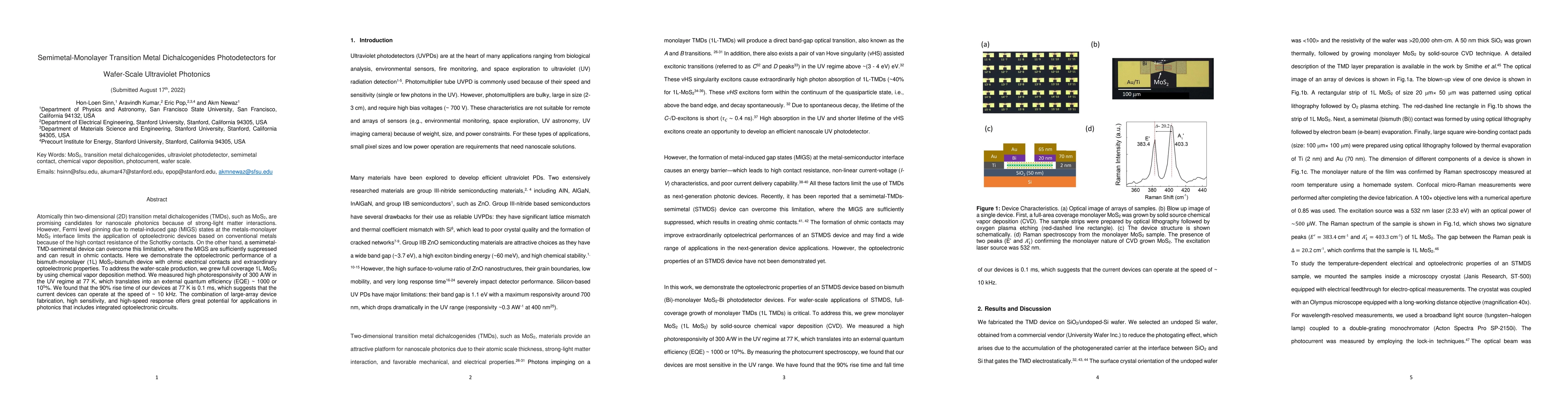
Atomically thin two-dimensional (2D) transition metal dichalcogenides (TMDs), such as MoS$_2$, are promising candidates for nanoscale photonics because of strong-light matter interactions. However, Fermi level pinning due to metal-induced gap (MIGS) states at the metals-monolayer MoS$_2$ interface limits the application of optoelectronic devices based on conventional metals because of the high contact resistance of the Schottky contacts. On the other hand, a semimetal-TMD-semimetal device can overcome this limitation, where the MIGS are sufficiently suppressed and can result in ohmic contacts. Here we demonstrate the optoelectronic performance of a bismuth-monolayer (1L) MoS$_2$-bismuth device with ohmic electrical contacts and extraordinary optoelectronic properties. To address the wafer-scale production, we grew full coverage 1L MoS$_2$ by using chemical vapor deposition method. We measured high photoresponsivity of 300 A/W in the UV regime at 77 K, which translates into an external quantum efficiency (EQE) ~ 1000 or $10^5$%. We found that the 90% rise time of our devices at 77 K is 0.1 ms, which suggests that the current devices can operate at the speed of ~ 10 kHz. The combination of large-array device fabrication, high sensitivity, and high-speed response offers great potential for applications in photonics that includes integrated optoelectronic circuits.
Get AI-generated insights about this paper's methodology, results, and significance.
Current paper (gray), citations (green), references (blue)
Duy-Nhat Ly, Dai-Nam Le, Van-Hoang Le et al.
Zihao Wang, Shaowei Li, Wan-Lu Li
Wenjun Zhang, Haotong Wang, Chengxiang Zhao et al.
Naoya Arakawa, Kenji Yonemitsu
Yongwoo Shin, Nikhil Sivadas
Title | Authors | Year | Actions |
---|---|---|---|
Noise‐Reduced WSe2 Phototransistors for Enhanced Photodetection Performance via Suppression of Metal‐Induced Gap States
|
Sunggyu Ryoo, Jinwoo Sim, Seungjun Jeong, Juntae Jang, Jaeyong Woo, Jaehyoung Park, Seongmin Ko, Yeeun Kim, Youngmin Song, Jongeun Yoo, Heebeom Ahn, Keehoon Kang, Daeheum Cho, Kyungjune Cho, Takhee Lee
|
2025
|
View Paper |
Waveguide-Coupled Light Photodetector Based on Two-Dimensional Molybdenum Disulfide
|
D. Hlushchenko, J. Olszewski, Tadeusz Martynkien, Michał Łukomski, Karolina Gemza, Paweł Karasiński, Magdalena Zięba, Tomasz Baraniecki, Ł. Duda, Alicja Bachmatiuk, Małgorzata Guzik, R. Kudrawiec
|
2024
|
View Paper |
Title | Authors | Year | Actions |
---|---|---|---|
Giant Effects of Interlayer Interaction on Valence-Band Splitting in Transition Metal Dichalcogenides
|
Garrett Benson, Viviane Zurdo Costa, N. Border, K. Yumigeta, Mark Blei, S. Tongay, K. Watanabe, T. Taniguchi, A. Ichimura, S. Kc, T. Salavati-fard, Bin Wang, A. Newaz
|
2022
|
View Paper |
Sub-200 Ω·µm Alloyed Contacts to Synthetic Monolayer MoS2
|
Aravindh Kumar, K. Schauble, Kathryn M. Neilson, A. Tang, P. Ramesh, H. Wong, E. Pop, K. Saraswat
|
2021
|
View Paper |
Epitaxial growth of wafer-scale molybdenum disulfide semiconductor single crystals on sapphire
|
Taotao Li, Wei Guo, Liang Ma, Weisheng Li, Zhihao Yu, Zhenyang Han, Si Gao, Lei Liu, D. Fan, Zixuan Wang, Yang Yang, Weiyi Lin, Zhongzhong Luo, Xiaoqing Chen, Ning Dai, X. Tu, D. Pan, Yagang Yao, Peng Wang, Y. Nie, Jinlan Wang, Yi Shi, Xinran Wang
|
2021
|
View Paper |
Ultralow contact resistance between semimetal and monolayer semiconductors
|
Pin-Chun Shen, C. Su, Y. Lin, Ang-Sheng Chou, Chao-Ching Cheng, Ji-Hoon Park, Ming-Hui Chiu, Ang-Yu Lu, Hao‐Ling Tang, M. Tavakoli, G. Pitner, X. Ji, Zhengyang Cai, Nannan Mao, Jiangtao Wang, V. Tung, Ju Li, J. Bokor, A. Zettl, Chih‐I Wu, T. Palacios, Lain‐Jong Li, Jing Kong
|
2021
|
View Paper |
Defects induced persistent photoconductivity in monolayer MoS2
|
Chandan, S. Sarkar, B. Angadi
|
2021
|
View Paper |
Benchmarking monolayer MoS2 and WS2 field-effect transistors
|
Amritanand Sebastian, Rahul Pendurthi, T. Choudhury, J. Redwing, Saptarshi Das
|
2021
|
View Paper |
Fast response photogating in monolayer MoS2 phototransistors.
|
D. Vaquero, V. Clericò, J. Salvador-Sánchez, E. Díaz, F. Dom'inguez-Adame, L. Chico, Y. Meziani, E. Diez, Jorge Quereda
|
2020
|
View Paper |
Ultrafast and broadband photodetectors based on a perovskite/organic bulk heterojunction for large-dynamic-range imaging
|
Chenglong Li, Hailu Wang, Fang Wang, Tengfei Li, Mengjian Xu, Hao Wang, Zhen Wang, X. Zhan, Weida Hu, Liang Shen
|
2020
|
View Paper |
Towards the evaluation of defects in MoS2 using cryogenic photoluminescence spectroscopy.
|
T. Verhagen, V. L. P. Guerra, G. Haider, M. Kalbáč, J. Vejpravová
|
2019
|
View Paper |
Monolithic integration of MoS2-based visible detectors and GaN-based UV detectors
|
You Wu, Zhiwen Li, K. Ang, Yuping Jia, Zhiming Shi, Zhi-Kai Huang, Wenjie Yu, Xiaojuan Sun, Xinke Liu, Dabing Li
|
2019
|
View Paper |
Origins of genuine Ohmic van der Waals contact between indium and MoS2
|
Bum-Kyu Kim, Tae-hyung Kim, Dong-Hwan Choi, Hanul Kim, Kenji Watanabe, T. Taniguchi, H. Rho, Ju-Jin Kim, Yong‐Hoon Kim, M. Bae
|
2019
|
View Paper |
MoS2 photodetectors integrated with photonic circuits
|
Juan Francisco Gonzalez Marin, D. Unuchek, Kenji Watanabe, T. Taniguchi, A. Kis
|
2019
|
View Paper |
Van der Waals contacts between three-dimensional metals and two-dimensional semiconductors
|
Yan Wang, Jong Chan Kim, R. Wu, Jenny Martinez, Xiuju Song, Jieun Yang, Fang Zhao, A. Mkhoyan, H. Jeong, M. Chhowalla
|
2019
|
View Paper |
Large-Area Ultraviolet Photodetectors Based on p-Type Multilayer MoS2 Enabled by Plasma Doping
|
Xiao-mei Zhang, Sian-Hong Tseng, M. Lu
|
2019
|
View Paper |
UV–Vis-NIR photodetector based on monolayer MoS2
|
Y. Zhou, Heishoku An, Cheng Gao, Zhaoqiang Zheng, Bing Wang
|
2019
|
View Paper |
Ultrahigh Performance of Self-Powered β-Ga2O3 Thin Film Solar-Blind Photodetector Grown on Cost-Effective Si Substrate Using High-Temperature Seed Layer
|
Kanika Arora, Neeraj Goel, Mahesh Kumar, Mukesh Kumar
|
2018
|
View Paper |
Approaching the Schottky–Mott limit in van der Waals metal–semiconductor junctions
|
Yuan Liu, Jian Guo, Enbo Zhu, L. Liao, Sung-Joon Lee, Mengning Ding, I. Shakir, V. Gambin, Yu Huang, X. Duan
|
2018
|
View Paper |
Via Method for Lithography Free Contact and Preservation of 2D Materials.
|
E. Telford, A. Benyamini, D. Rhodes, Da Wang, Younghun Jung, A. Zangiabadi, Kenji Watanabe, T. Taniguchi, S. Jia, K. Barmak, A. Pasupathy, C. Dean, J. Hone
|
2018
|
View Paper |
Wafer-Scale Growth and Transfer of Highly-Oriented Monolayer MoS2 Continuous Films.
|
Hua Yu, Mengzhou Liao, Wenjuan Zhao, Guodong Liu, X. Zhou, Zheng Wei, Xiaozhi Xu, Kaihui Liu, Zhiwei Hu, K. Deng, Shuyun Zhou, Jin-an Shi, Lin Gu, Cheng Shen, Tingting Zhang, Luojun Du, Luojun Du, Li Xie, Jianqi Zhu, Wei Chen, Rong Yang, D. Shi, Guangyu Zhang
|
2017
|
View Paper |
Photogating in Low Dimensional Photodetectors
|
Hehai Fang, Weida Hu
|
2017
|
View Paper |
Large array fabrication of high performance monolayer MoS2 photodetectors
|
A. E. Yore, K. Smithe, Sauraj Jha, K. Ray, E. Pop, Abul K M Newaz
|
2017
|
View Paper |
2D transition metal dichalcogenides
|
Sajedeh Manzeli, D. Ovchinnikov, D. Pasquier, O. Yazyev, A. Kis
|
2017
|
View Paper |
Photoresponse of Natural van der Waals Heterostructures.
|
K. Ray, A. E. Yore, Tong Mou, Sauraj Jha, K. Smithe, Bin Wang, E. Pop, A. Newaz
|
2017
|
View Paper |
Junction-Structure-Dependent Schottky Barrier Inhomogeneity and Device Ideality of Monolayer MoS2 Field-Effect Transistors.
|
B. Moon, G. Han, H. Kim, Homin Choi, J. Bae, Jaesu Kim, Youngjo Jin, H. Jeong, Min-Kyu Joo, Young Hee Lee, S. Lim
|
2017
|
View Paper |
High-Field Transport and Velocity Saturation in Synthetic Monolayer MoS2.
|
K. Smithe, C. English, S. Suryavanshi, E. Pop
|
2017
|
View Paper |
Slow cooling and efficient extraction of C-exciton hot carriers in MoS2 monolayer
|
Lei Wang, Zhuo Wang, Hai‐Yu Wang, G. Grinblat, Yuli Huang, Dan Wang, X. Ye, Xianbin Li, Q. Bao, A. Wee, S. Maier, Qidai Chen, M. Zhong, C. Qiu, Hongbo Sun
|
2017
|
View Paper |
A review on mechanics and mechanical properties of 2D materials—Graphene and beyond
|
D. Akinwande, Christopher J. Brennan, J. Bunch, P. Egberts, J. Felts, Huajian Gao, Rui Huang, Joon-Seok Kim, Teng Li, Yao Li, K. Liechti, Nanshu Lu, Harold S. Park, E. Reed, Peng Wang, B. Yakobson, Teng Zhang, Yongwei Zhang, Yao Zhou, Yong Zhu
|
2016
|
View Paper |
Highly sensitive visible to infrared MoTe2 photodetectors enhanced by the photogating effect
|
Hai Huang, Jianlu Wang, Weida Hu, L. Liao, Peng Wang, Xudong Wang, Fan Gong, Yan Chen, Guangjian Wu, Wenjin Luo, H. Shen, Tie Lin, Jinglan Sun, Xiangjian Meng, Xiaoshuang Chen, J. Chu
|
2016
|
View Paper |
InGaAs Nanomembrane/Si van der Waals Heterojunction Photodiodes with Broadband and High Photoresponsivity.
|
D. Um, Youngsu Lee, Seongdong Lim, Jonghwa Park, Wen-Chun Yen, Y. Chueh, Hyung-jun Kim, Hyunhyub Ko
|
2016
|
View Paper |
Intrinsic electrical transport and performance projections of synthetic monolayer MoS2 devices
|
K. Smithe, C. English, S. Suryavanshi, E. Pop
|
2016
|
View Paper |
Photonics and optoelectronics of 2D semiconductor transition metal dichalcogenides
|
K. Mak, J. Shan
|
2016
|
View Paper |
Two-dimensional transition metal dichalcogenides as atomically thin semiconductors: opportunities and challenges.
|
Xidong Duan, Chen Wang, A. Pan, R. Yu, Xiangfeng Duan
|
2015
|
View Paper |
Gate Controlled Photocurrent Generation Mechanisms in High-Gain In₂Se₃ Phototransistors.
|
J. Island, Sofya I. Blanter, M. Buscema, H. V. D. Zant, A. Castellanos-Gómez
|
2015
|
View Paper |
Highly Sensitive, Encapsulated MoS2 Photodetector with Gate Controllable Gain and Speed.
|
D. Kufer, G. Konstantatos
|
2015
|
View Paper |
Ultrafast Intrinsic Photoresponse and Direct Evidence of Sub-gap States in Liquid Phase Exfoliated MoS2Thin Films
|
S. Ghosh, A. Winchester, B. Muchharla, Milinda Wasala, S. Feng, A. Elías, M. Krishna, T. Harada, C. Chin, K. Dani, S. Kar, M. Terrones, S. Talapatra
|
2015
|
View Paper |
Extrinsic Origin of Persistent Photoconductivity in Monolayer MoS2 Field Effect Transistors
|
Yueh-Chun Wu, Cheng-Hua Liu, Shao-Yu Chen, F. Shih, Po-Hsun Ho, Chun-Wei Chen, C. Liang, Wei-Hua Wang
|
2015
|
View Paper |
Large-Area Epitaxial Monolayer MoS2
|
D. Dumcenco, D. Ovchinnikov, K. Marinov, P. Lazic, M. Gibertini, N. Marzari, Oriol López Sánchez, Yen‐Cheng Kung, Daria Krasnozhon, Ming-Wei Chen, Simone Bertolazzi, P. Gillet, A. Fontcuberta i Morral, A. Radenović, A. Kis
|
2015
|
View Paper |
Exciton radiative lifetimes in two-dimensional transition metal dichalcogenides.
|
M. Palummo, M. Bernardi, J. Grossman
|
2015
|
View Paper |
Photogating of mono- and few-layer MoS2
|
B. Miller, E. Parzinger, Anna Vernickel, A. Holleitner, U. Wurstbauer
|
2015
|
View Paper |
On-chip Fabrication of High Performance Nanostructured ZnO UV Detectors
|
M. Alenezi, M. Alenezi, S. Henley, S. Silva
|
2015
|
View Paper |
Nanoscale ultraviolet photodetectors based on onedimensional metal oxide nanostructures
|
Wei Tian, Hao Lu, Liang Li
|
2015
|
View Paper |
Highly Sensitive Ultraviolet Photodetectors Fabricated from ZnO Quantum Dots/Carbon Nanodots Hybrid Films
|
D. Guo, C. Shan, Song-nan Qu, D. Shen
|
2014
|
View Paper |
High‐Performance Flexible Broadband Photodetector Based on Organolead Halide Perovskite
|
Xin Hu, Xiaodong Zhang, Lin Liang, Jian Bao, Shuang Li, Wenlong Yang, Yi Xie
|
2014
|
View Paper |
Two-dimensional material nanophotonics
|
F. Xia, Han Wang, Di Xiao, M. Dubey, A. Ramasubramaniam
|
2014
|
View Paper |
Radiative lifetimes of excitons and trions in monolayers of the metal dichalcogenide MoS 2
|
Haining Wang, Changjian Zhang, Weimin Chan, C. Manolatou, S. Tiwari, F. Rana
|
2014
|
View Paper |
Controllable Schottky Barriers between MoS2 and Permalloy
|
Weiyi Wang, Yanwen Liu, Lei Tang, Yibo Jin, Tongtong Zhao, F. Xiu
|
2014
|
View Paper |
Mechanisms of photoconductivity in atomically thin MoS2.
|
M. Furchi, D. Polyushkin, A. Pospischil, T. Mueller
|
2014
|
View Paper |
Graphene photodetectors with ultra-broadband and high responsivity at room temperature.
|
Chang-Hua Liu, You-Chia Chang, T. Norris, Z. Zhong
|
2014
|
View Paper |
Probing excitonic states in suspended two-dimensional semiconductors by photocurrent spectroscopy
|
A. Klots, A. Newaz, A. Newaz, Bin Wang, Bin Wang, Dhiraj Prasai, H. Krzyżanowska, Junhao Lin, Junhao Lin, D. Caudel, N. Ghimire, N. Ghimire, Jiaqiang Yan, Jiaqiang Yan, B. Ivanov, K. Velizhanin, A. Burger, D. Mandrus, D. Mandrus, N. Tolk, S. Pantelides, S. Pantelides, K. Bolotin
|
2014
|
View Paper |
Fast and broadband photoresponse of few-layer black phosphorus field-effect transistors.
|
M. Buscema, D. Groenendijk, Sofya I. Blanter, G. Steele, H. V. D. van der Zant, A. Castellanos-Gómez
|
2014
|
View Paper |
Emerging device applications for semiconducting two-dimensional transition metal dichalcogenides.
|
Deep Jariwala, V. Sangwan, L. Lauhon, T. Marks, M. Hersam
|
2014
|
View Paper |
Electronic transport and device prospects of monolayer molybdenum disulphide grown by chemical vapour deposition
|
Wenjuan Zhu, T. Low, Yi‐Hsien Lee, Han Wang, D. Farmer, J. Kong, F. Xia, P. Avouris
|
2014
|
View Paper |
Optical spectrum of MoS2: many-body effects and diversity of exciton states.
|
D. Qiu, Felipe H. da Jornada, S. Louie
|
2013
|
View Paper |
Low‐Cost Fully Transparent Ultraviolet Photodetectors Based on Electrospun ZnO‐SnO2 Heterojunction Nanofibers
|
Wei Tian, T. Zhai, Chao Zhang, Song-Lin Li, Xi Wang, Fei Liu, Dequan Liu, X. Cai, K. Tsukagoshi, D. Golberg, Y. Bando
|
2013
|
View Paper |
Observation of trap-assisted space charge limited conductivity in short channel MoS2 transistor
|
S. Ghatak, A. Ghosh
|
2013
|
View Paper |
Ultraviolet Photodetector Fabricated From Multiwalled Carbon Nanotubes/Zinc-Oxide Nanowires/p-GaN Composite Structure
|
Dali Shao, Mingpeng Yu, J. Lian, S. Sawyer
|
2013
|
View Paper |
A Comprehensive Review of Semiconductor Ultraviolet Photodetectors: From Thin Film to One-Dimensional Nanostructures
|
L. Sang, M. Liao, M. Sumiya
|
2013
|
View Paper |
Self-Powered ZnO Nanowire UV Photodetector Integrated With GaInP/GaAs/Ge Solar Cell
|
Jei-Li Hou, S. Chang, Chih-Hung Wu, T. Hsueh
|
2013
|
View Paper |
Ultrasensitive photodetectors based on monolayer MoS2.
|
Oriol Lopez-Sanchez, D. Lembke, M. Kayci, A. Radenović, A. Kis
|
2013
|
View Paper |
Strong Light-Matter Interactions in Heterostructures of Atomically Thin Films
|
L. Britnell, R. Ribeiro, A. Eckmann, R. Jalil, B. Belle, A. Mishchenko, Y.J. Kim, R. Gorbachev, T. Georgiou, S. Morozov, A. Grigorenko, A.K. Geim, C. Casiraghi, A. H. Castro Neto, K. Novoselov
|
2013
|
View Paper |
Piezo-phototronic effect enhanced visible/UV photodetector of a carbon-fiber/ZnO-CdS double-shell microwire.
|
Fang Zhang, Simiao Niu, Wenxi Guo, G. Zhu, Y. Liu, Xiaoling Zhang, Zhong Lin Wang
|
2013
|
View Paper |
Tunable graphene-silicon heterojunctions for ultrasensitive photodetection.
|
Xiaohong An, Fangze Liu, Y. Jung, S. Kar
|
2013
|
View Paper |
Photoresponse mechanisms of ultraviolet photodetectors based on colloidal ZnO quantum dot-graphene nanocomposites
|
D. Son, H. Yang, Tae Whan Kim, W. Park
|
2013
|
View Paper |
Electronics and optoelectronics of two-dimensional transition metal dichalcogenides.
|
Qing Hua Wang, K. Kalantar-zadeh, A. Kis, J. Coleman, M. Strano
|
2012
|
View Paper |
Electron-hole transport and photovoltaic effect in gated MoS2 Schottky junctions
|
M. Fontana, Tristan Deppe, A. Boyd, M. Rinzan, A. Liu, M. Paranjape, P. Barbara
|
2012
|
View Paper |
Middle-ultraviolet-enhanced photodetectors based on Mg0.4Zn0.6O/ZnO homojunction with a high selectivity for 300 nm around light
|
Yongdan Zhu, Hai Zhou, G. Fang, Meiya Li
|
2012
|
View Paper |
Graphene/ZnO nanowire/graphene vertical structure based fast-response ultraviolet photodetector
|
Xuewen Fu, Z. Liao, Yangbo Zhou, Han-Chun Wu, Ya‐Qing Bie, Jun Xu, Dapeng Yu
|
2012
|
View Paper |
An Optimized Ultraviolet‐A Light Photodetector with Wide‐Range Photoresponse Based on ZnS/ZnO Biaxial Nanobelt
|
Linfeng Hu, Jian Yan, M. Liao, H. Xiang, X. Gong, Lide Zhang, X. Fang
|
2012
|
View Paper |
ZnO nanorods grown on polymer substrates as UV photodetectors
|
I. Yao, T. Tseng, P. Lin
|
2012
|
View Paper |
Comparative Study of Silicon-Based Ultraviolet Photodetectors
|
Lei Shi, S. Nihtianov
|
2012
|
View Paper |
Photoconductivity of biased graphene
|
M. Freitag, T. Low, F. Xia, P. Avouris
|
2012
|
View Paper |
Hybrid graphene-quantum dot phototransistors with ultrahigh gain.
|
G. Konstantatos, M. Badioli, L. Gaudreau, J. Osmond, M. Bernechea, P. G. D. Arquer, F. Gatti, F. Koppens
|
2011
|
View Paper |
Nature of electronic states in atomically thin MoS₂ field-effect transistors.
|
S. Ghatak, A. N. Pal, A. Ghosh
|
2011
|
View Paper |
A three-dimensional vertically aligned functionalized multilayer graphene architecture: an approach for graphene-based thermal interfacial materials.
|
Q. Liang, Xuxia Yao, Wei Wang, Yan Liu, C. Wong
|
2011
|
View Paper |
ZnO-Paper Based Photoconductive UV Sensor
|
A. J. Gimenez, J. Yáñez-Limón, J. Seminario
|
2011
|
View Paper |
High responsivity ultraviolet photodetector realized via a carrier-trapping process
|
Jinchang Liu, C. Shan, B. Li, Z. Zhang, Chu-Shou Yang, D. Shen, X. Fan
|
2010
|
View Paper |
ZnO-Based Ultraviolet Photodetectors
|
Kewei Liu, M. Sakurai, M. Aono
|
2010
|
View Paper |
Emerging photoluminescence in monolayer MoS2.
|
A. Splendiani, Liangyan Sun, Yuanbo Zhang, Tianshu Li, Jonghwan Kim, C. Chim, G. Galli, Feng Wang
|
2010
|
View Paper |
Determination of the parameters for the back-to-back switched Schottky barrier structures
|
M. Ahmetoğlu, S. Akay
|
2010
|
View Paper |
Solar Cells, Photodetectors, and Optical Sources from Infrared Colloidal Quantum Dots
|
E. Sargent
|
2008
|
View Paper |
Solution-processed ultraviolet photodetectors based on colloidal ZnO nanoparticles.
|
Yizheng Jin, Jianpu Wang, Baoquan Sun, J. Blakesley, N. Greenham
|
2008
|
View Paper |
Wide bandgap UV photodetectors: a short review of devices and applications
|
F. Omnès, E. Monroy, E. Muñoz, J. Reverchon
|
2007
|
View Paper |
Novel broadband photodetector for optical communication
|
A. Dutta, M. Islam
|
2005
|
View Paper |
Nanoscale spatial phase modulation of GaN on a V-grooved Si Substrate-cubic phase GaN on Si(001) for monolithic integration
|
S.C. Lee, B. Pattada, S. Hersee, Ying-Bing Jiang, S. Brueck
|
2005
|
View Paper |
Perceptual Ability with Real-World Nighttime Scenes: Image-Intensified, Infrared, and Fused-Color Imagery
|
E. Essock, M. Sinai, J. McCarley, W. K. Krebs, J. DeFord
|
1999
|
View Paper |
Trapping of minority carriers in multicrystalline silicon
|
D. Macdonald, A. Cuevas
|
1999
|
View Paper |
Effects of electron confinement on thermionic emission current in a modulation doped heterostructure
|
A. Anwar, B. Nabet, J. Culp, F. Castro
|
1999
|
View Paper |
Growth and applications of Group III-nitrides
|
O. Ambacher
|
1998
|
View Paper |
On the physics of metal-semiconductor interfaces
|
W. Monch
|
1990
|
View Paper |
Schottky barriers and semiconductor band structures.
|
J. Tersoff
|
1985
|
View Paper |
The metal-semiconductor interface: Si (111) and zincblende (110) junctions
|
C. Tejedor, F. Flores, E. Louis
|
1977
|
View Paper |
Trapping of Minority Carriers in Silicon. I. P -Type Silicon
|
J. A. Hornbeck, J. R. Haynes
|
1955
|
View Paper |
Effect of Traps on Carrier Injection in Semiconductors
|
H. Y. Fan
|
1953
|
View Paper |
Temporary Traps in Silicon and Germanium
|
J. R. Haynes, J. A. Hornbeck
|
1953
|
View Paper |
2023 The Authors
|
2017
|
||
Recent advances in ultraviolet photodetectors
|
Z. Alaie, S. Nejad, M. Yousefi
|
2015
|
View Paper |
Quality Improvement of GaN on Si Substrate for Ultraviolet Photodetector Application
|
Chao-Wei Hsu, Yung-Feng Chen, Y. Su
|
2014
|
View Paper |
Atomically Thin MoS2: A New DirectGap Semiconductor
|
2010
|
||
Supporting Information
|
Arelo O. A Tanoh, Nicolas Gauriot, G. Delport, James Xiao, Rajal Pandya, Jooyoung Sung, Jesse, Allardice, Zhaojun Li, Cyan A. Williams, Alan Baldwin, S. Stranks, A. Rao
|
2005
|
View Paper |
Control of structural defects in group III–V–N alloys grown on Si
|
Hiroo Yonezu
|
2002
|
View Paper |
Photocurrent as we illuminate the sample and terminate the illumination. The measurement was conducted at 77 K. The photocurrent was measured by a digital multimeter
|
2000
|
||
Semiconductor ultraviolet detectors
|
M. Razeghia, A. Rogalskib
|
1996
|
View Paper |
C: Solid State Phys
|
|||
Neto, K
|
|||
S1 94305, USA 4 Precourt Institute for Energy, Stanford University, Stanford, California 94305, USA
|
|||
Transition Metal Dichalcogenides Photodetectors for Wafer-Scale Ultraviolet Photonics Hon
|
Showing first page preview. Click "Open Full PDF" to view the complete paper.
Your comment contains inappropriate language and has been rejected.
Are you sure you want to remove this tag? This action cannot be undone.
Someone just favorited a paper!
Comments (0)