Academic Profile
Statistics
Similar Authors
Papers on arXiv
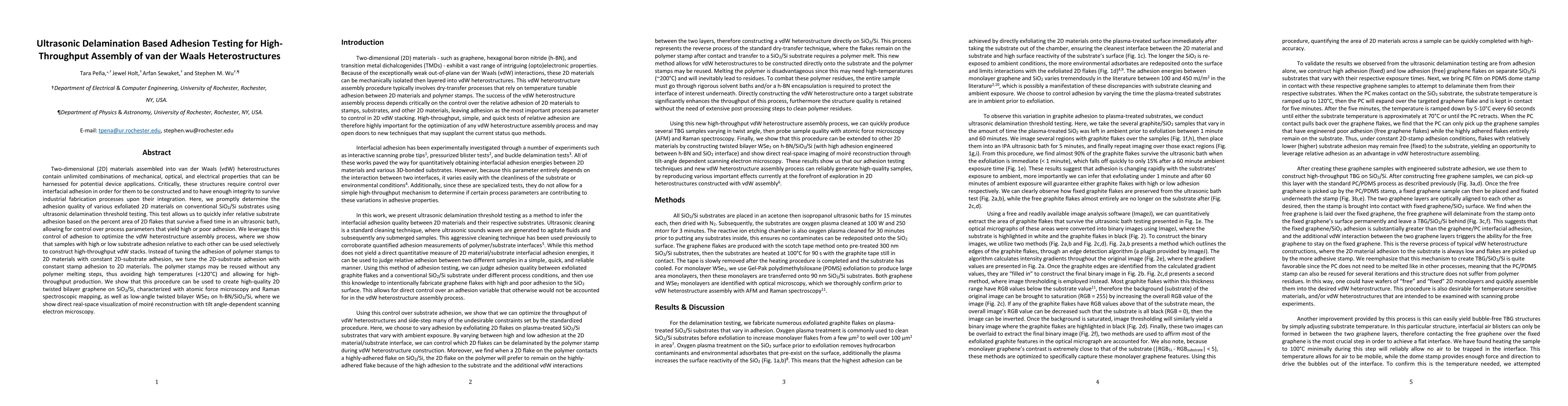
Two-dimensional (2D) materials assembled into van der Waals (vdW) heterostructures contain unlimited combinations of mechanical, optical, and electrical properties that can be harnessed for potentia...
We demonstrate a method to induce tensile and compressive strain into two-dimensional transition metal dichalcogenide (TMDC) MoS$_{2}$ via the deposition of stressed thin films to encapsulate exfoli...
The primary mechanism of operation of almost all transistors today relies on electric-field effect in a semiconducting channel to tune its conductivity from the conducting 'on'-state to a non-conduc...
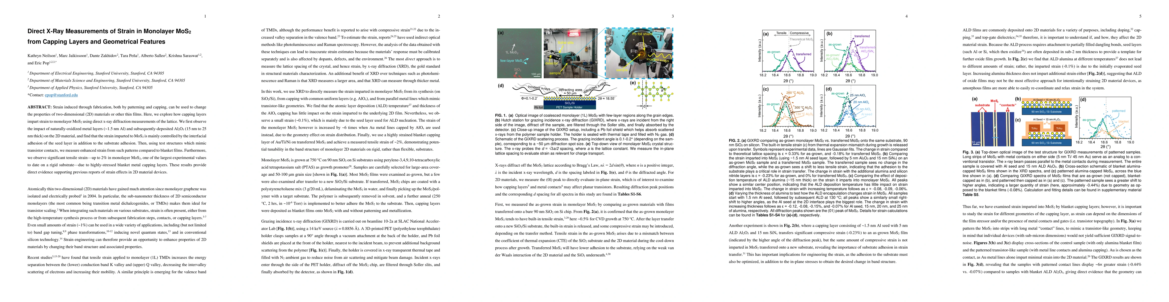
Strain induced through fabrication, both by patterning and capping, can be used to change the properties of two-dimensional (2D) materials or other thin films. Here, we explore how capping layers impa...
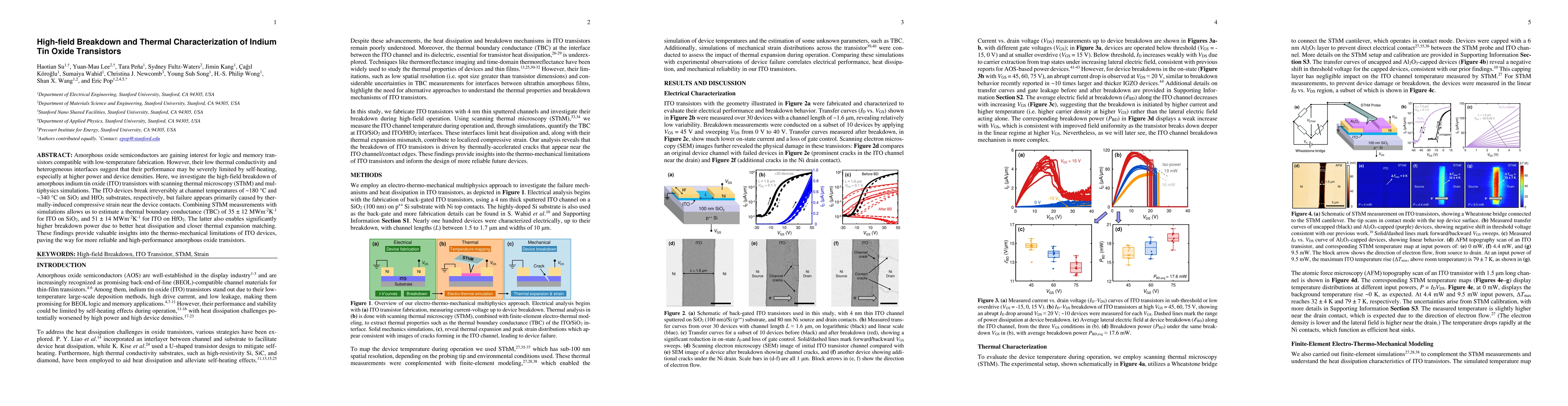
Amorphous oxide semiconductors are gaining interest for logic and memory transistors compatible with low-temperature fabrication. However, their low thermal conductivity and heterogeneous interfaces s...
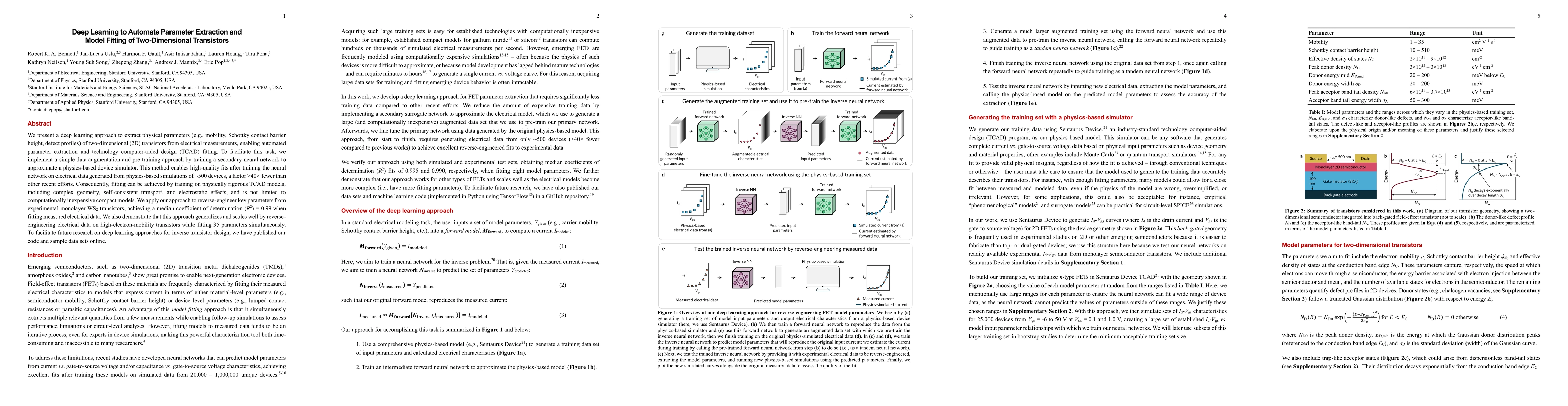
We present a deep learning approach to extract physical parameters (e.g., mobility, Schottky contact barrier height, defect profiles) of two-dimensional (2D) transistors from electrical measurements, ...
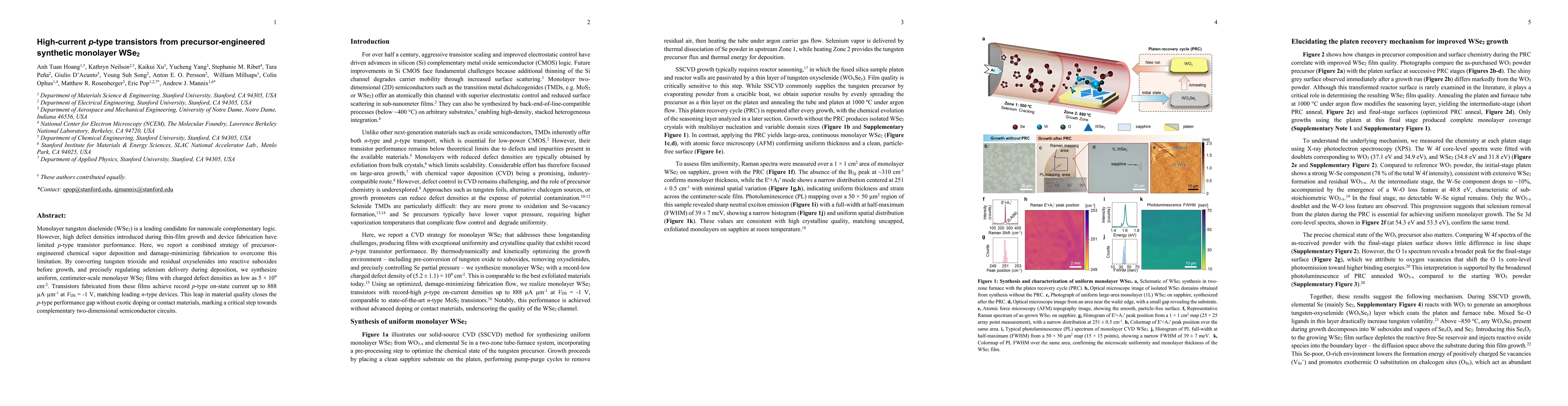
Monolayer tungsten diselenide (WSe$_2$) is a leading candidate for nanoscale complementary logic. However, high defect densities introduced during thin-film growth and device fabrication have limited ...
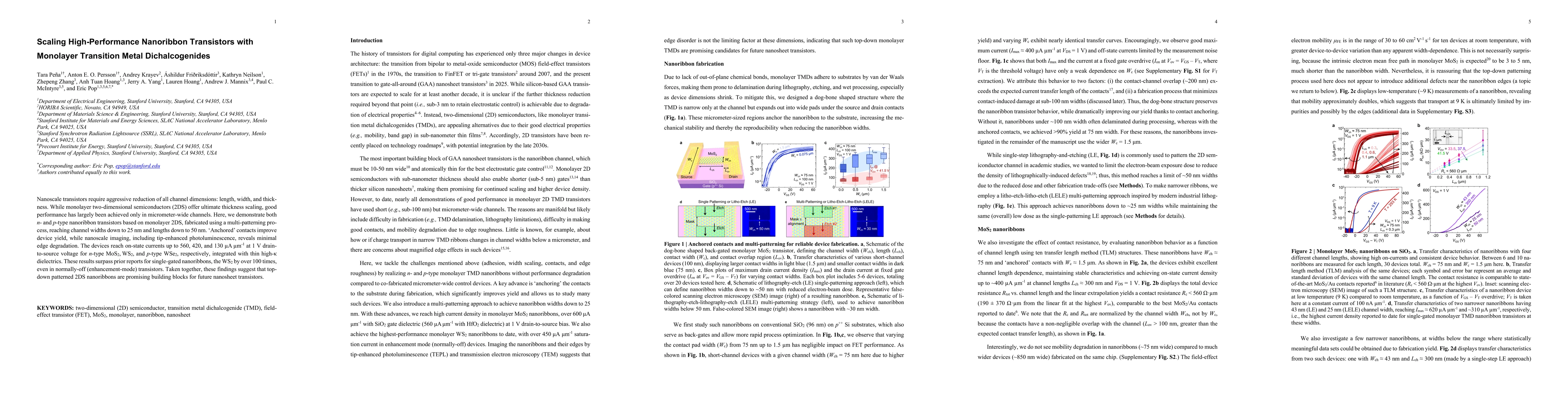
Nanoscale transistors require aggressive reduction of all channel dimensions: length, width, and thickness. While monolayer two-dimensional semiconductors (2DS) offer ultimate thickness scaling, good ...
Two-dimensional (2D) materials with a twist between layers exhibit a moir\'e interference pattern with larger periodicity than any of the constituent layer unit cells. In these systems, a wealth of ex...
We demonstrate a gate dielectric engineering approach leveraging an ultrathin, atomic layer deposited (ALD) silicon oxide interfacial layer (SiL) between the amorphous oxide semiconductor (AOS) channe...
As we move beyond the era of transistor miniaturization, back-end-of-line-compatible transistors that can be stacked monolithically in the third dimension promise improved performance for low-power el...