Academic Profile
Statistics
Similar Authors
Papers on arXiv
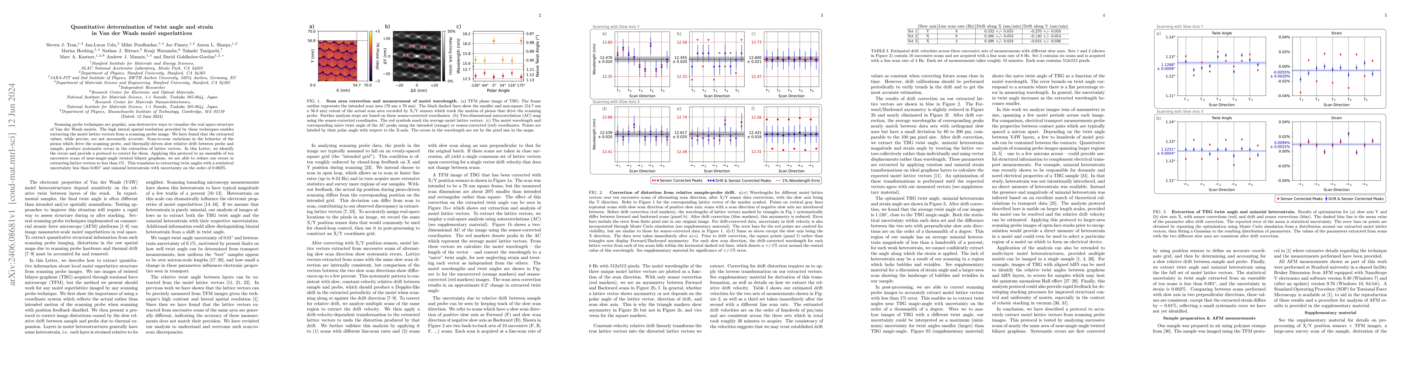
Scanning probe techniques are popular, non-destructive ways to visualize the real space structure of Van der Waals moir\'es. The high lateral spatial resolution provided by these techniques enables ...
The electronic properties of moir\'e heterostructures depend sensitively on the relative orientation between layers of the stack. For example, near-magic-angle twisted bilayer graphene (TBG) commonl...
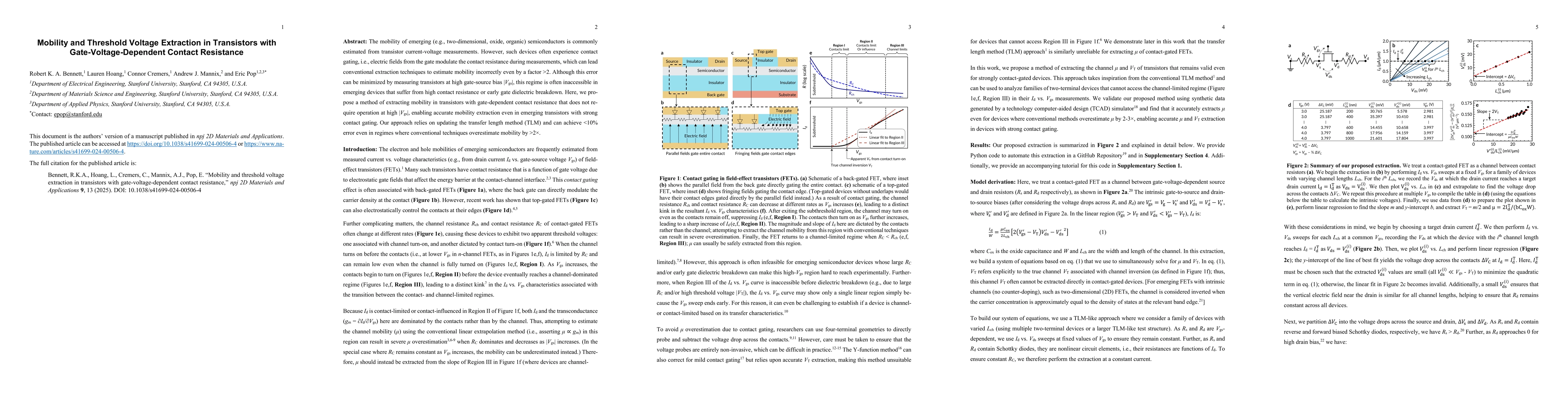
The mobility of emerging (e.g., two-dimensional, oxide, organic) semiconductors is commonly estimated from transistor current-voltage measurements. However, such devices often experience contact gat...
New properties can arise at van der Waals (vdW) interfaces hosting a moir\'e pattern generated by interlayer twist and strain. However, achieving precise control of interlayer twist/strain remains a...
Two-dimensional (2D) semiconducting transition-metal dichalcogenides (TMDCs) are an exciting platform for new excitonic physics and next-generation electronics, creating a strong demand to understan...
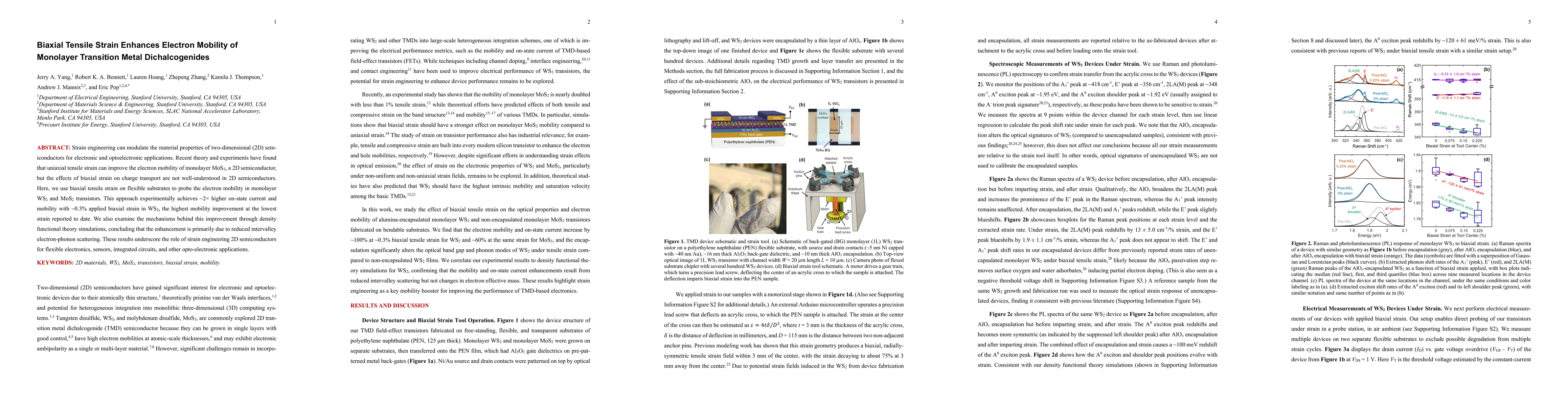
Strain engineering can modulate the material properties of two-dimensional (2D) semiconductors for electronic and optoelectronic applications. Recent theory and experiments have found that uniaxial ...
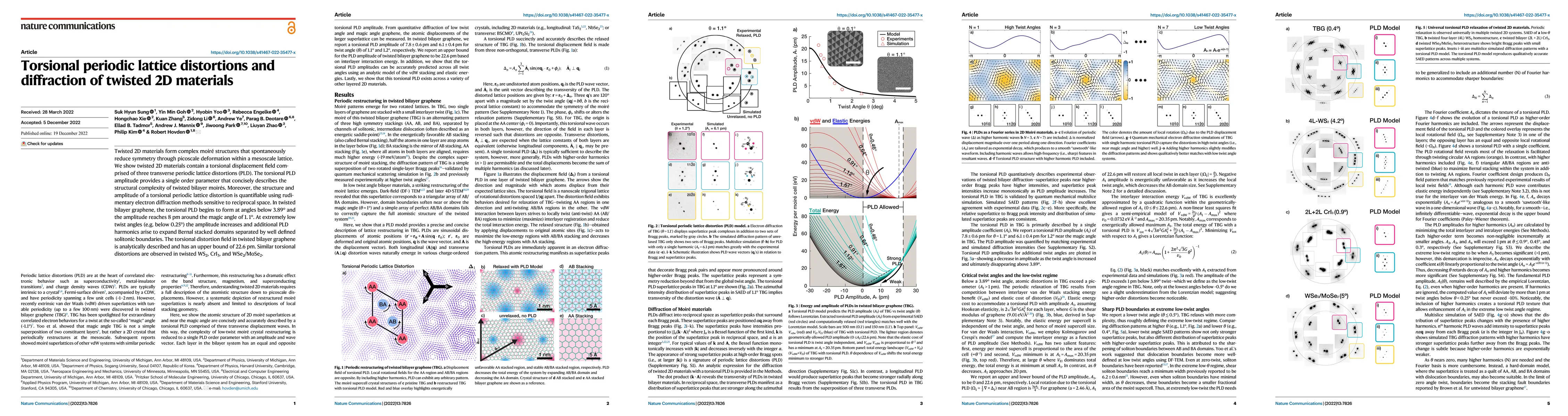
Twisted 2D materials form complex moir\'e structures that spontaneously reduce symmetry through picoscale deformation within a mesoscale lattice. We show twisted 2D materials contain a torsional dis...
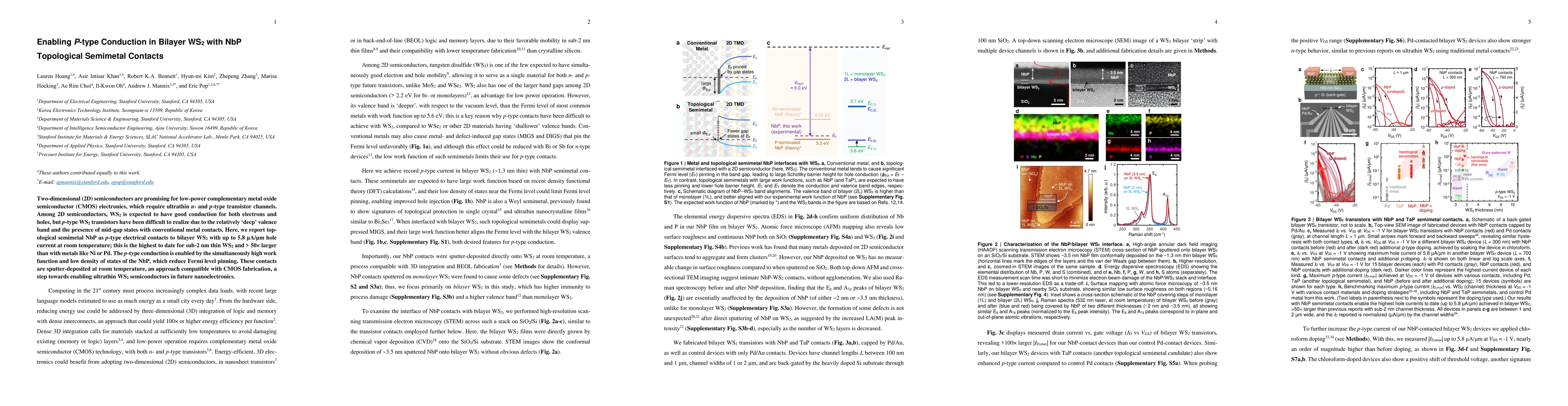
Two-dimensional (2D) semiconductors are promising for low-power complementary metal oxide semiconductor (CMOS) electronics, which require ultrathin n- and p-type transistor channels. Among 2D semicond...
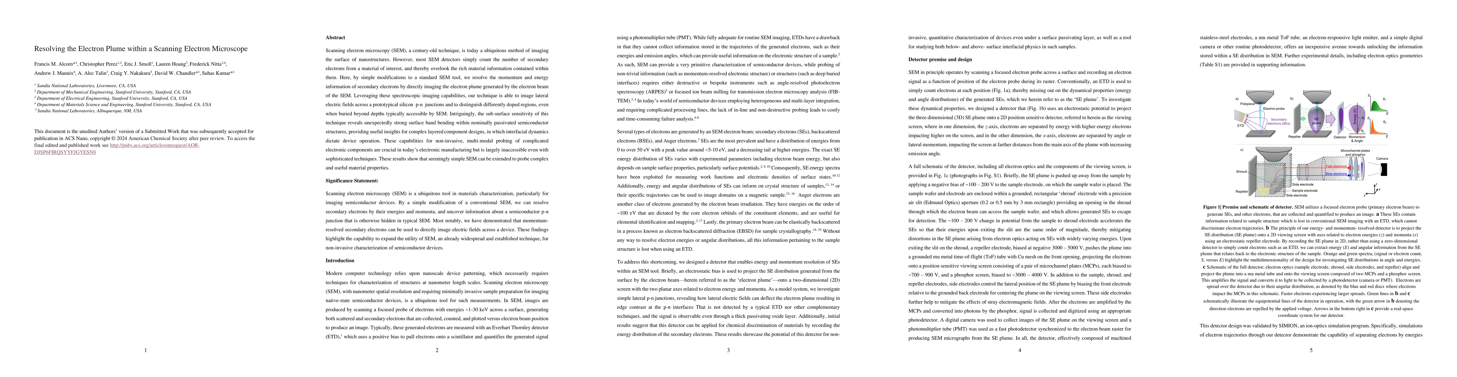
Scanning electron microscopy (SEM), a century-old technique, is today a ubiquitous method of imaging the surface of nanostructures. However, most SEM detectors simply count the number of secondary ele...
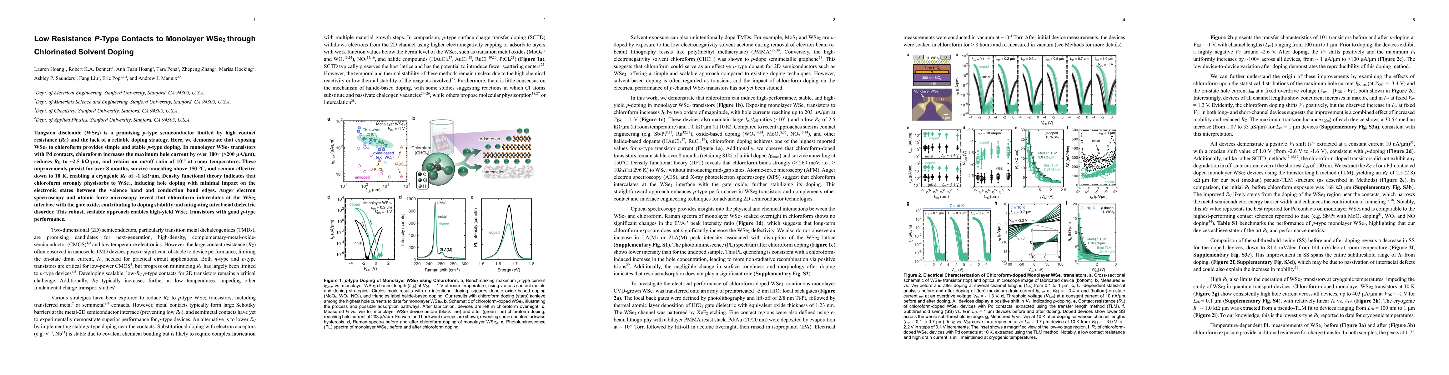
Tungsten diselenide (WSe$_2$) is a promising p-type semiconductor limited by high contact resistance ($R_\textrm{C}$) and the lack of a reliable doping strategy. Here, we demonstrate that exposing WSe...
Two-dimensional (2D) Janus transition metal dichalcogenides (TMDs) are promising candidates for various applications in non-linear optics, energy harvesting, and catalysis. These materials are usually...
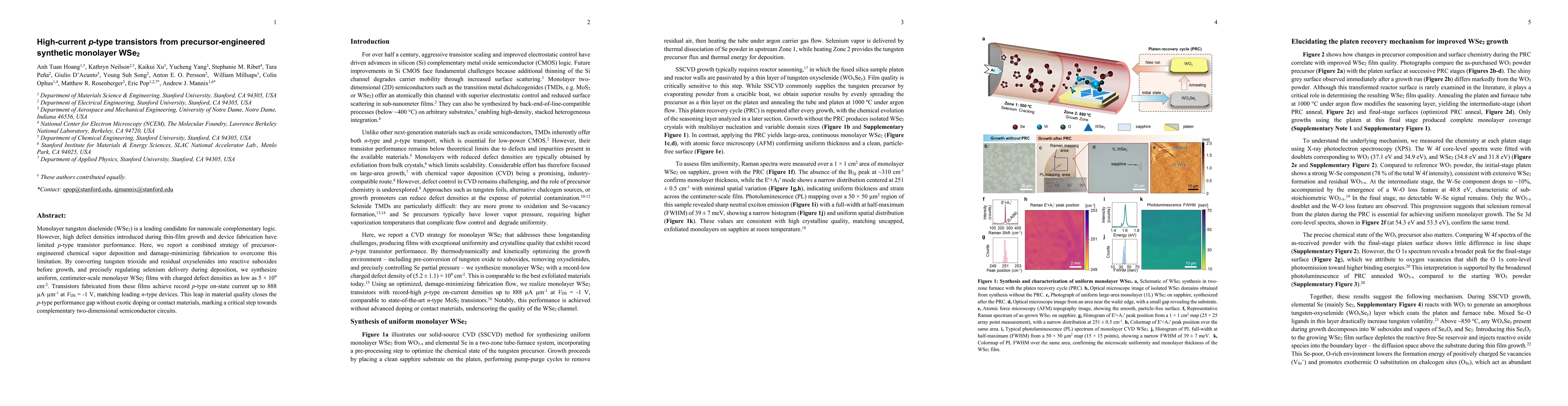
Electronic and optoelectronic applications of two-dimensional (2D) semiconductors demand precise control over material quality, including thickness, composition, doping, and defect density. Convention...
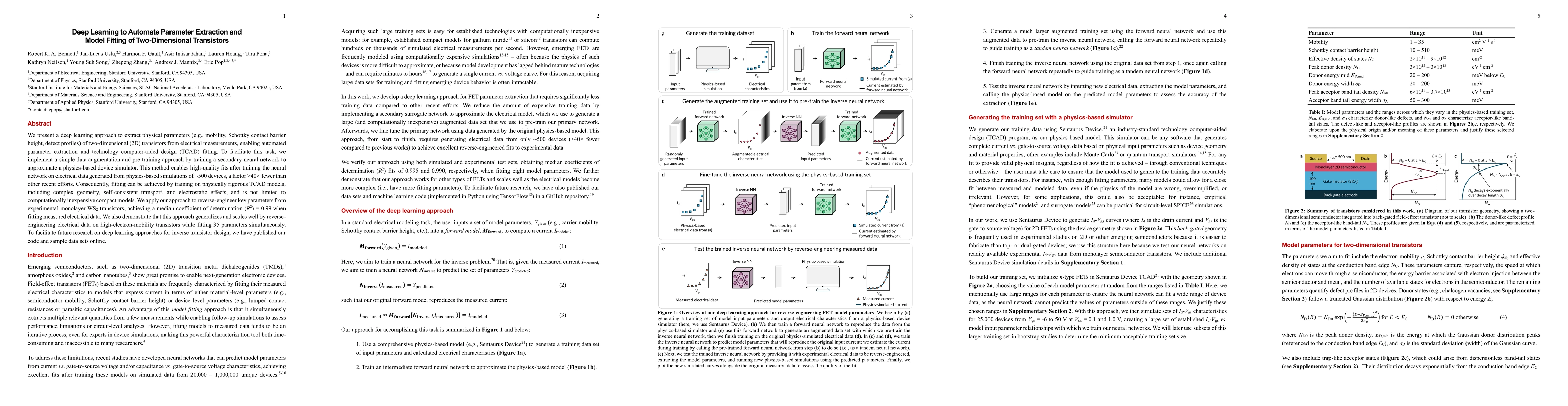
We present a deep learning approach to extract physical parameters (e.g., mobility, Schottky contact barrier height, defect profiles) of two-dimensional (2D) transistors from electrical measurements, ...
Monolayer tungsten diselenide (WSe$_2$) is a leading candidate for nanoscale complementary logic. However, high defect densities introduced during thin-film growth and device fabrication have limited ...
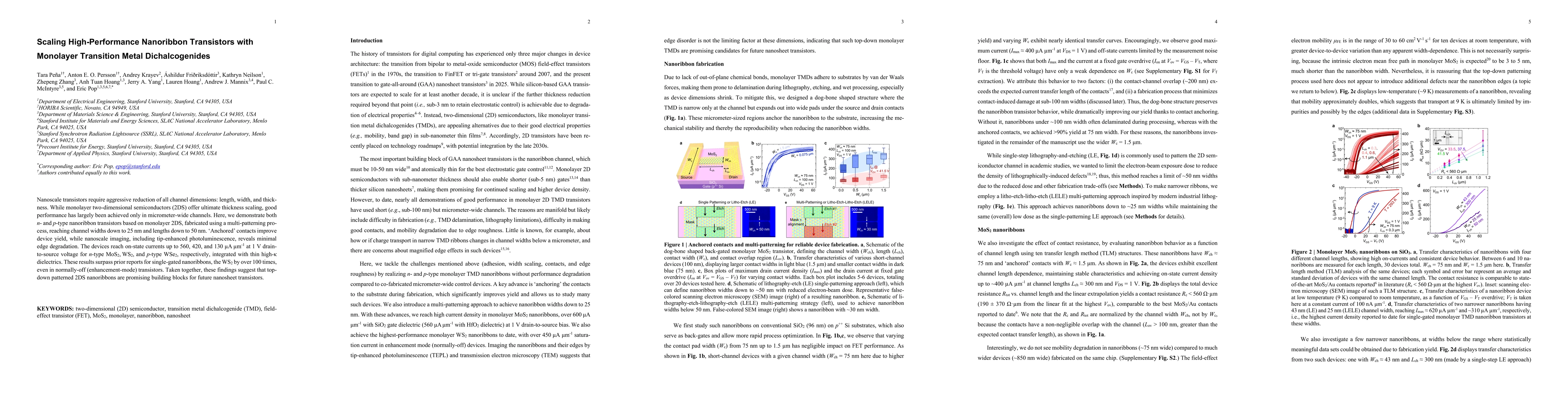
Nanoscale transistors require aggressive reduction of all channel dimensions: length, width, and thickness. While monolayer two-dimensional semiconductors (2DS) offer ultimate thickness scaling, good ...
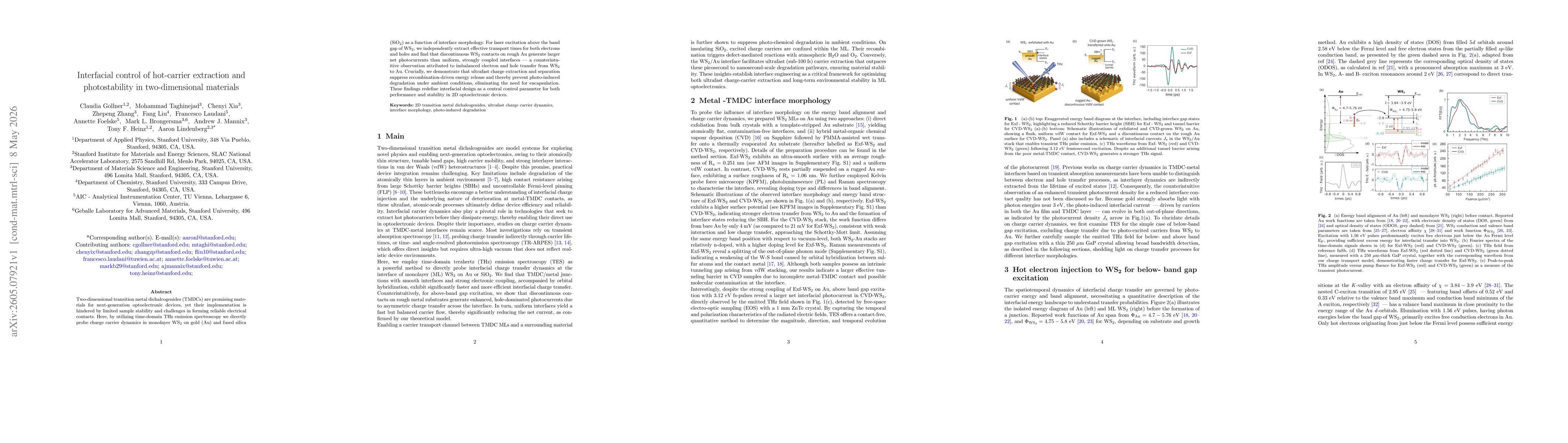
Two-dimensional transition metal dichalcogenides (TMDCs) are promising materials for next-generation optoelectronic devices, yet their implementation is hindered by limited sample stability and challe...
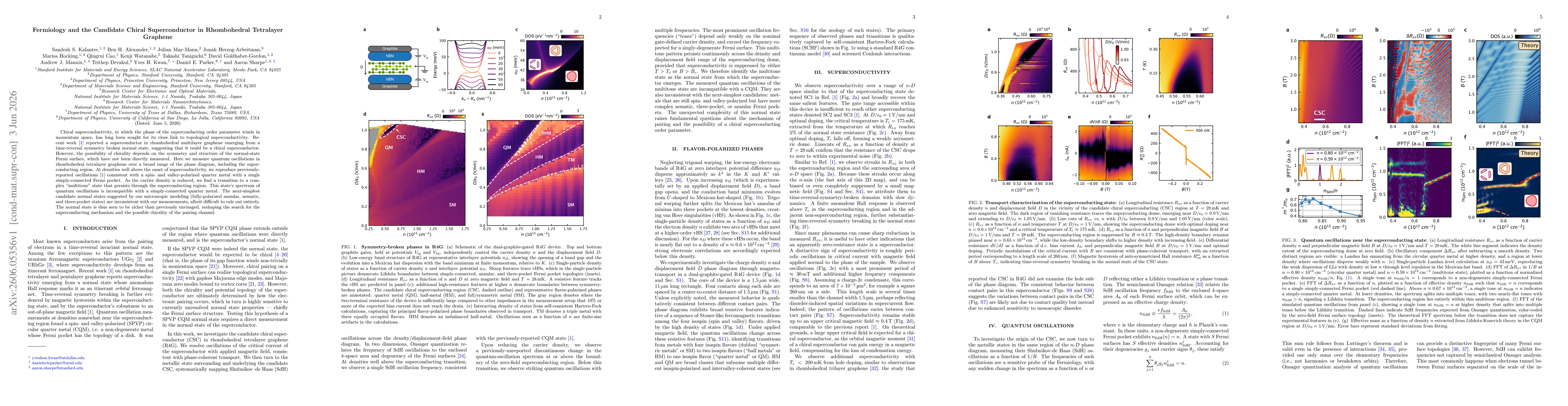
Chiral superconductivity, in which the phase of the superconducting order parameter winds in momentum space, has long been sought for its close link to topological superconductivity. Recent work repor...