Publication
Metrics
AI Quick Summary
This paper details a modified SEM technique that resolves momentum and energy information of secondary electrons, enabling imaging of lateral electric fields and distinguishing differently doped regions in silicon p-n junctions. The method reveals unexpected surface band bending, providing insights for complex layered semiconductor designs.
Paper Preview
Abstract
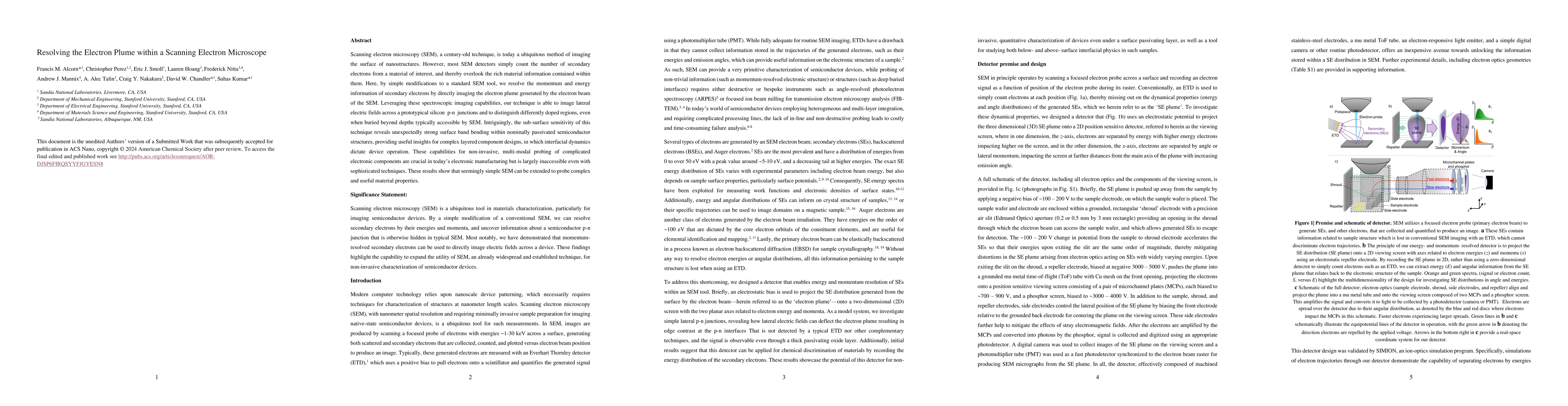
Scanning electron microscopy (SEM), a century-old technique, is today a ubiquitous method of imaging the surface of nanostructures. However, most SEM detectors simply count the number of secondary electrons from a material of interest, and thereby overlook the rich material information contained within them. Here, by simple modifications to a standard SEM tool, we resolve the momentum and energy information of secondary electrons by directly imaging the electron plume generated by the electron beam of the SEM. Leveraging these spectroscopic imaging capabilities, our technique is able to image lateral electric fields across a prototypical silicon p-n junctions and to distinguish differently doped regions, even when buried beyond depths typically accessible by SEM. Intriguingly, the sub-surface sensitivity of this technique reveals unexpectedly strong surface band bending within nominally passivated semiconductor structures, providing useful insights for complex layered component designs, in which interfacial dynamics dictate device operation. These capabilities for non-invasive, multi-modal probing of complicated electronic components are crucial in today's electronic manufacturing but is largely inaccessible even with sophisticated techniques. These results show that seemingly simple SEM can be extended to probe complex and useful material properties.
AI Key Findings
Get AI-generated insights about this paper's methodology, results, significance, and more — seven facets brought into focus.
Impact
Paper Details
Authors
PDF Preview
Citation Network
Current paper (gray), citations (green), references (blue)
Display is limited for performance on very large graphs.
Discussion 0