Academic Profile
Statistics
Similar Authors
Papers on arXiv
In the recent past, MnTe has proven to be a crucial component of the intrinsic magnetic topological insulator (IMTI) family [MnTe]m[Bi2Te3]n, which hosts a wide range of magneto-topological properti...
Scaling up superconducting quantum circuits based on transmon qubits necessitates substantial enhancements in qubit coherence time. Among the materials considered for transmon qubits, tantalum (Ta) ...
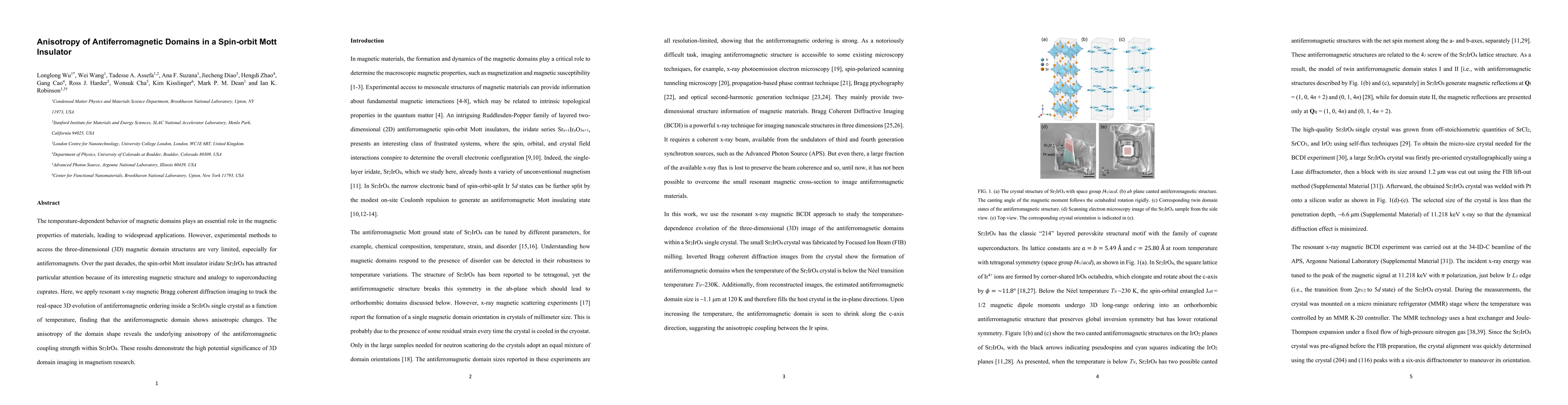
The temperature-dependent behavior of magnetic domains plays an essential role in the magnetic properties of materials, leading to widespread applications. However, experimental methods to access th...
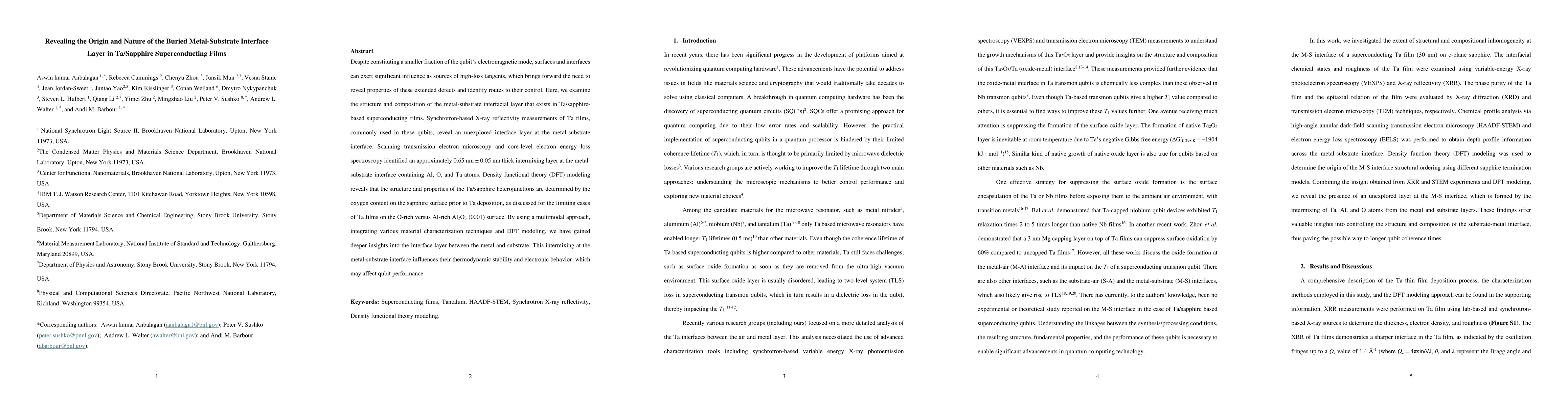
The performance of superconducting quantum circuits for quantum computing has advanced tremendously in recent decades; however, a comprehensive understanding of relaxation mechanisms does not yet ex...
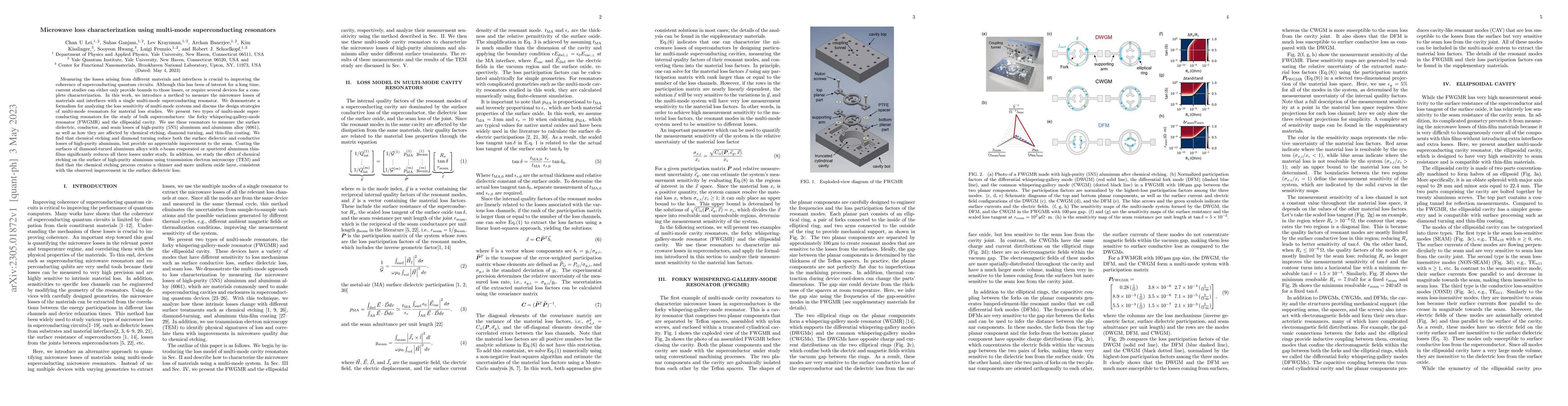
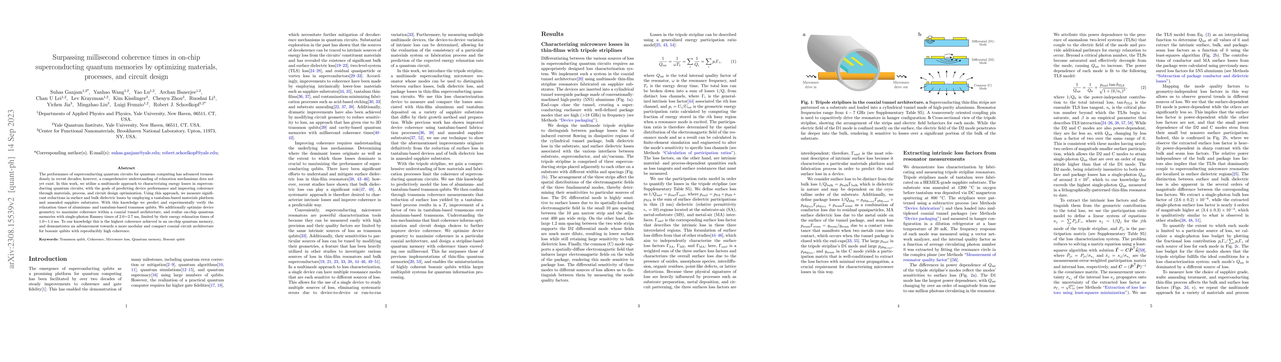
Measuring the losses arising from different materials and interfaces is crucial to improving the coherence of superconducting quantum circuits. Although this has been of interest for a long time, cu...
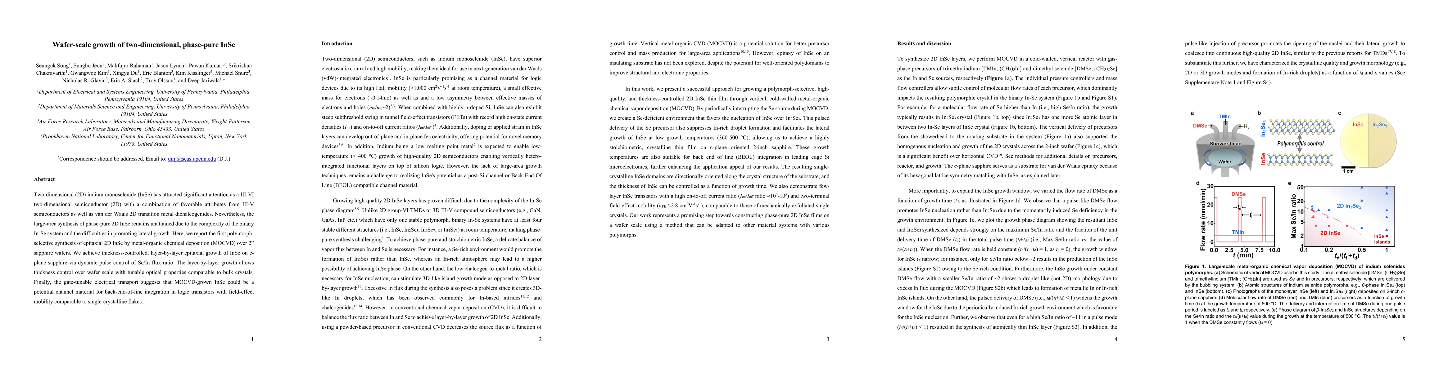
Two-dimensional (2D) indium monoselenide (InSe) has attracted significant attention as a III-VI two-dimensional semiconductor (2D) with a combination of favorable attributes from III-V semiconductor...
Over the past decades, superconducting qubits have emerged as one of the leading hardware platforms for realizing a quantum processor. Consequently, researchers have made significant effort to under...
Transparent contact interfaces in superconductor-graphene hybrid systems are critical for realizing superconducting quantum applications. Here, we examine the effect of the edge-contact fabrication ...
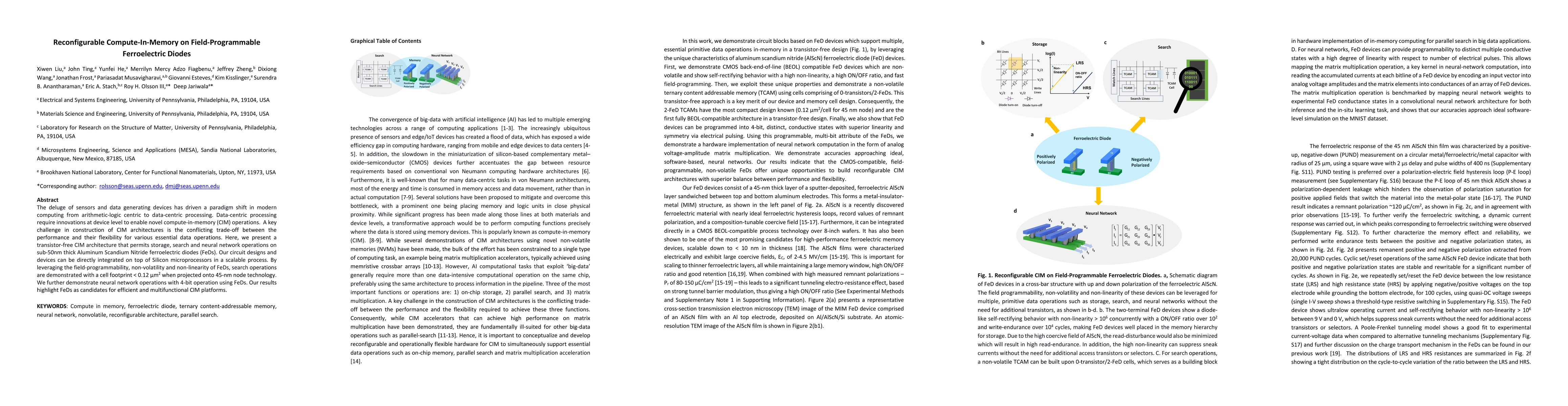
The deluge of sensors and data generating devices has driven a paradigm shift in modern computing from arithmetic-logic centric to data centric processing. At a hardware level, this presents an urge...
The semiconductor-metal junction is one of the most critical factors for high performance electronic devices. In two-dimensional (2D) semiconductor devices, minimizing the voltage drop at this junct...

Previous efforts to directly write conductive metals have been narrowly focused on nanoparticle ink suspensions that require aggressive sintering (>200 {\deg}C) and result in low-density, small-grai...
Dispersionless flat bands are proposed to be a fundamental ingredient to achieve the various sought after quantum states of matter including high-temperature superconductivity1-4 and fractional quan...
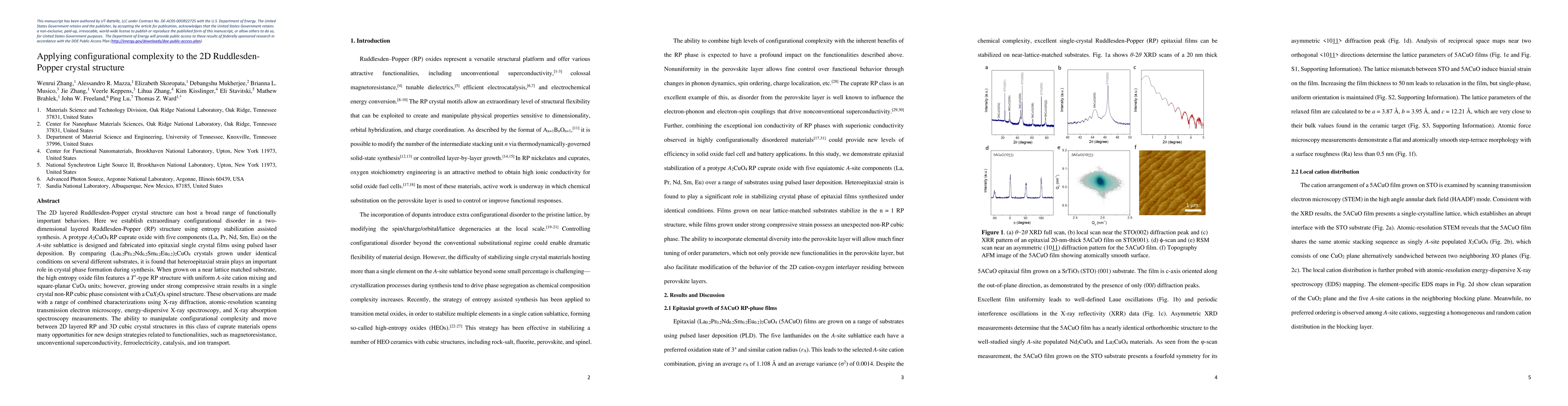
The 2D layered Ruddlesden-Popper crystal structure can host a broad range of functionally important behaviors. Here we establish extraordinary configurational disorder in a two dimensional layered R...
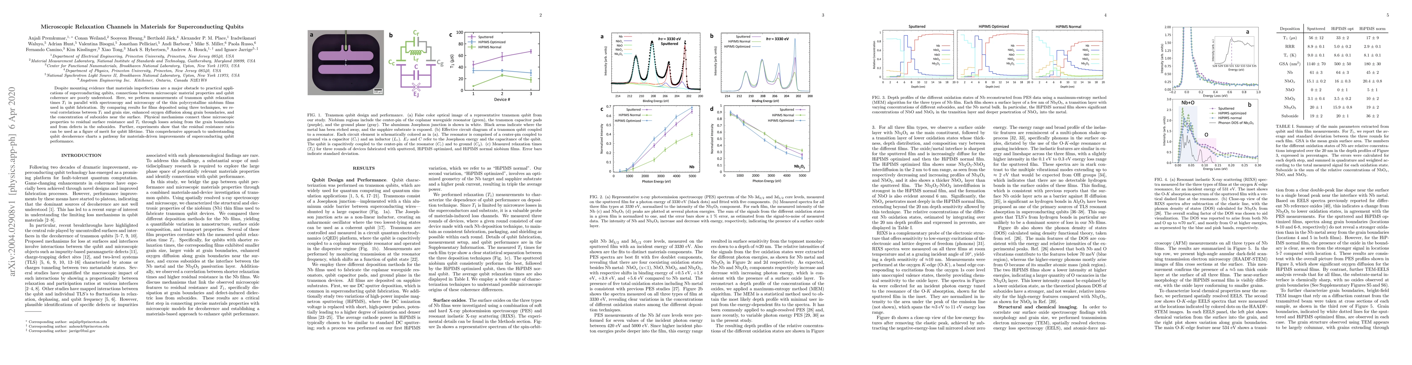
Despite mounting evidence that materials imperfections are a major obstacle to practical applications of superconducting qubits, connections between microscopic material properties and qubit coheren...
Despite constituting a smaller fraction of the qubits electromagnetic mode, surfaces and interfaces can exert significant influence as sources of high-loss tangents, which brings forward the need to r...
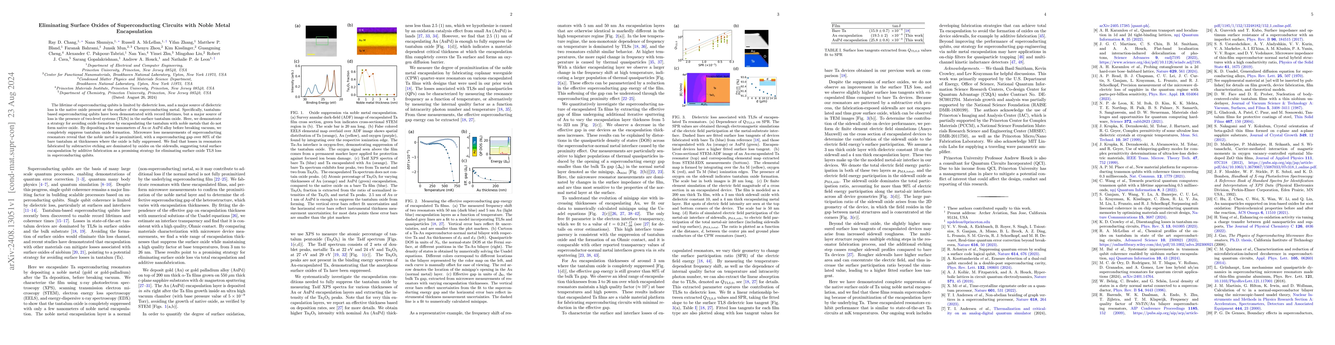
The lifetime of superconducting qubits is limited by dielectric loss, and a major source of dielectric loss is the native oxide present at the surface of the superconducting metal. Specifically, tanta...
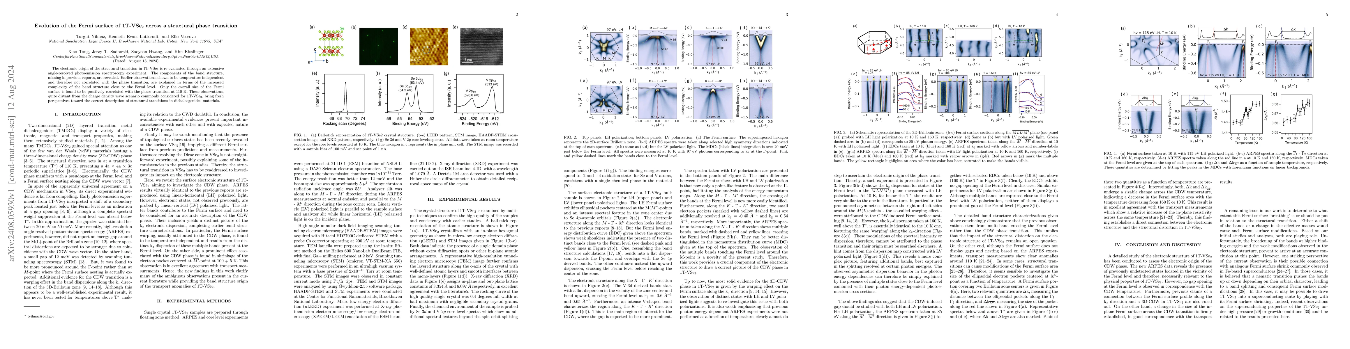
The electronic origin of the structural transition in 1T-VSe$_2$ is re-evaluated through an extensive angle-resolved photoemission spectroscopy experiment. The components of the band structure, missin...
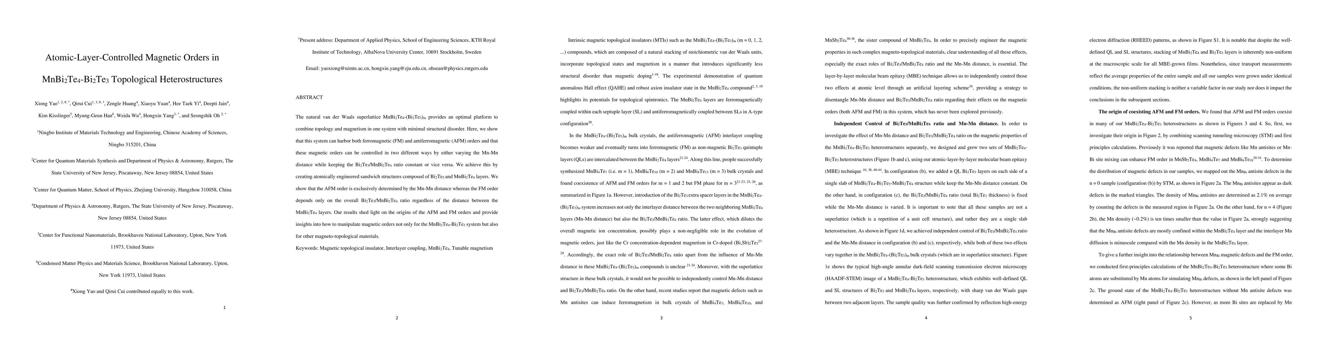
The natural van der Waals superlattice MnBi2Te4-(Bi2Te3)m provides an optimal platform to combine topology and magnetism in one system with minimal structural disorder. Here, we show that this system ...
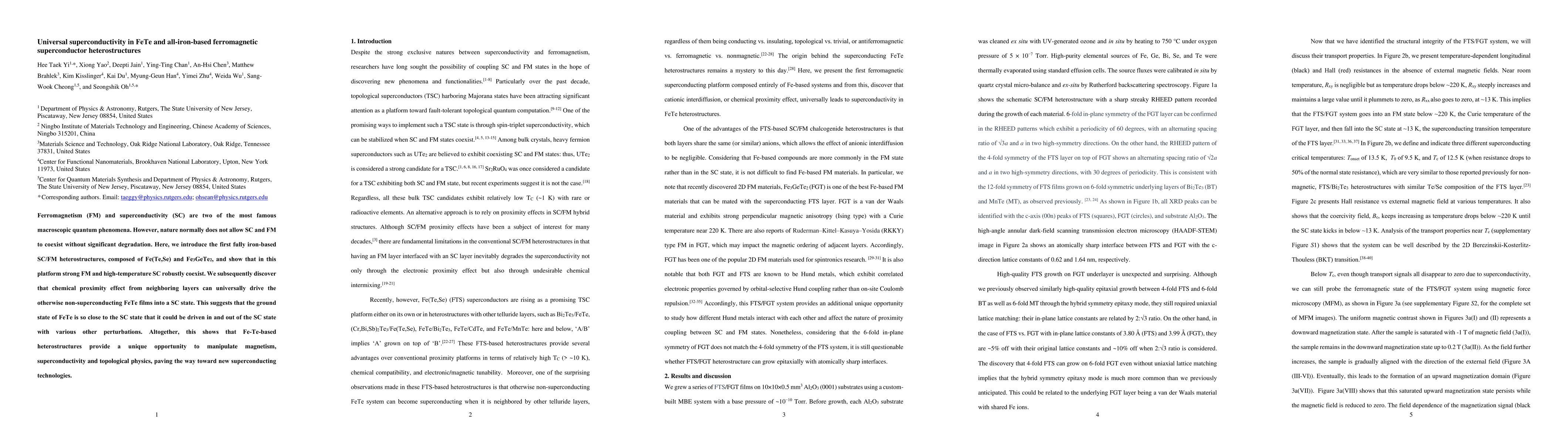
Ferromagnetism (FM) and superconductivity (SC) are two of the most famous macroscopic quantum phenomena. However, nature normally does not allow SC and FM to coexist without significant degradation. H...
![Thumbnail for Single-layer magnet phase in intrinsic magnetic topological insulators,
$[\mathrm{MnTe}][\mathrm{Bi}_{2}\mathrm{Te}_{3}]_{\mathrm{n}}$, far beyond
the thermodynamic limit](https://nbg1.your-objectstorage.com/arxivlens/thumbnails/2503.06283.webp)
The intrinsic magnetic topological insulator (IMTI) family $[\mathrm{MnTe}][\mathrm{Bi}_{2}\mathrm{Te}_{3}]_{\mathrm{n}}$ has demonstrated magneto-topological properties dependent on $n$, making it a ...
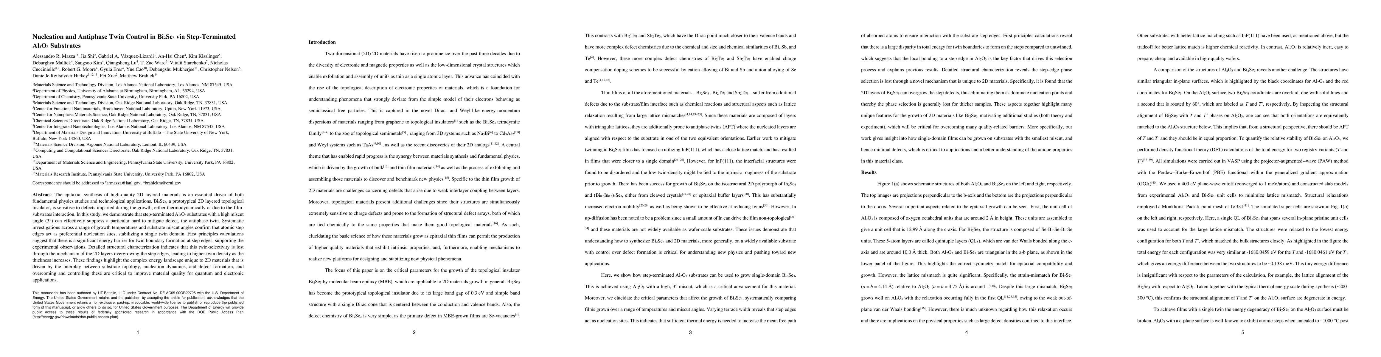
The epitaxial synthesis of high-quality 2D layered materials is an essential driver of both fundamental physics studies and technological applications. Bi$_2$Se$_3$, a prototypical 2D layered topologi...
Crystal engineering is a method for discovering new quantum materials and phases, which may be achieved by external pressure or strain. Chemical pressure is unique in that it generates internal pressu...
Controlling spin currents, i.e., the flow of spin angular momentum, in small magnetic devices is the principal objective of spin electronics, a main contender for future energy efficient information t...
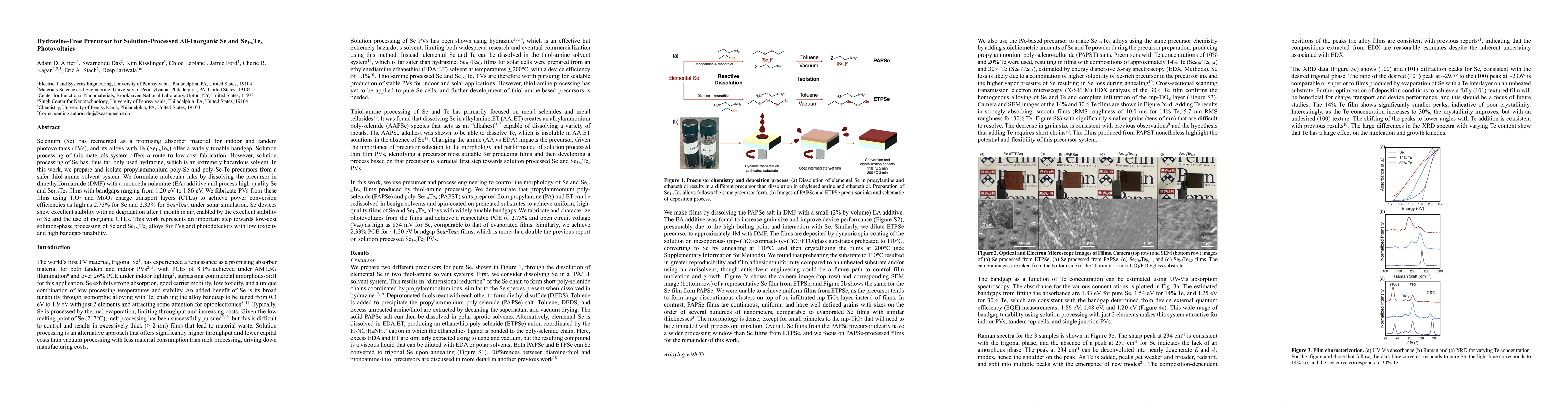
Selenium (Se) has reemerged as a promising absorber material for indoor and tandem photovoltaics (PVs), and its alloys with Te (Se1-xTex) offer a widely tunable bandgap. Solution processing of this ma...
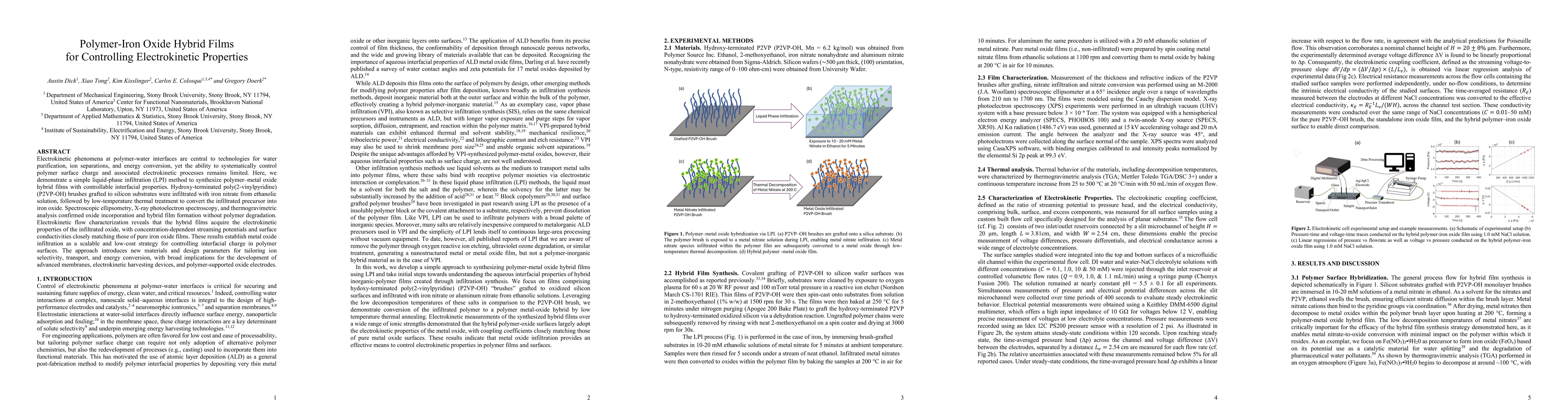
Electrokinetic phenomena at polymer-water interfaces are central to technologies for water purification, ion separations, and energy conversion, yet the ability to systematically control polymer surfa...
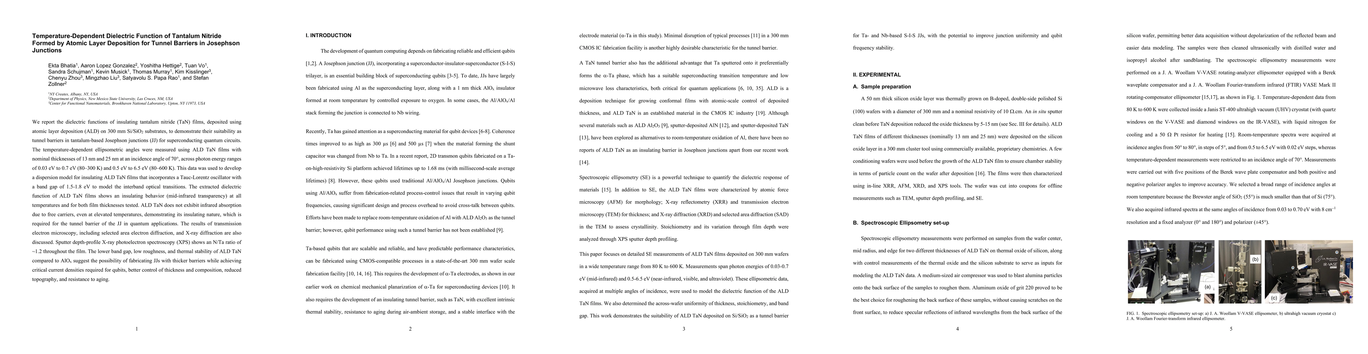
We report the dielectric functions of insulating tantalum nitride (TaN) films, deposited using atomic layer deposition (ALD) on 300 mm Si/SiO2 substrates, to demonstrate their suitability as tunnel ba...
Dielectric loss arising from two-level systems (TLS) at surfaces and interfaces remains a primary limitation to coherence in superconducting transmon qubits. Niobium (Nb), a widely used material in su...