Quick Summary:

This paper reports the first polymorph-selective synthesis of epitaxial 2D InSe using metal-organic chemical deposition over 2-inch sapphire wafers, achieving thickness-controlled, layer-by-layer epitaxial growth with tunable optical properties and potential for logic transistor applications.

Summary

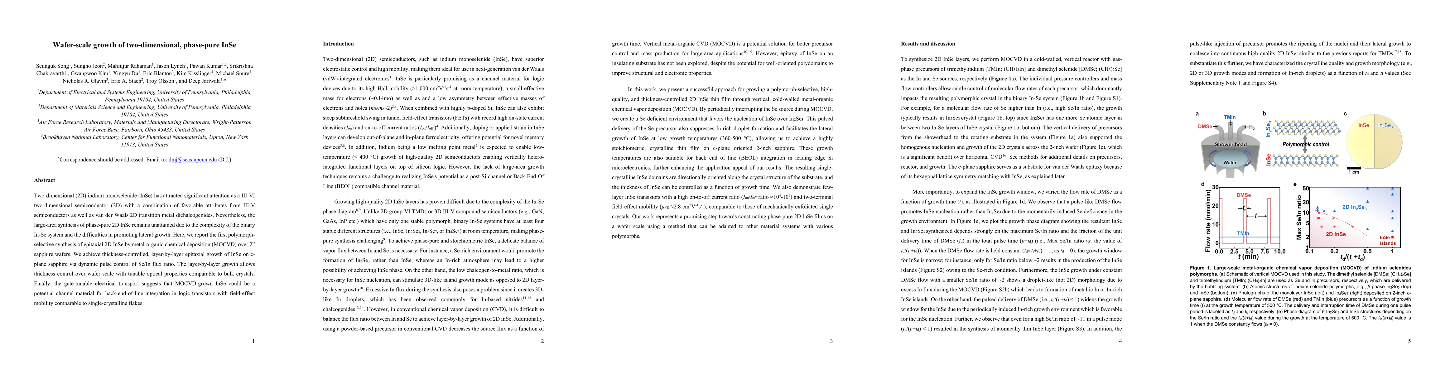
Two-dimensional (2D) indium monoselenide (InSe) has attracted significant attention as a III-VI two-dimensional semiconductor (2D) with a combination of favorable attributes from III-V semiconductors as well as van der Waals 2D transition metal dichalcogenides. Nevertheless, the large-area synthesis of phase-pure 2D InSe remains unattained due to the complexity of the binary In-Se system and the difficulties in promoting lateral growth. Here, we report the first polymorph-selective synthesis of epitaxial 2D InSe by metal-organic chemical deposition (MOCVD) over 2 inch diameter sapphire wafers. We achieve thickness-controlled, layer-by-layer epitaxial growth of InSe on c-plane sapphire via dynamic pulse control of Se/In flux ratio. The layer-by-layer growth allows thickness control over wafer scale with tunable optical properties comparable to bulk crystals. Finally, the gate-tunable electrical transport suggests that MOCVD-grown InSe could be a potential channel material for back-end-of-line integration in logic transistors with field-effect mobility comparable to single-crystalline flakes.

AI Key Findings

Get AI-generated insights about this paper's methodology, results, and significance.

Paper Details

PDF Preview

Download PDF

Key Terms

layer (0.228)
growth (0.218)
thickness (0.217)
tunable (0.214)
synthesis (0.214)
iii (0.191)
comparable (0.186)
metal (0.183)
control (0.148)
der (0.145)
lateral (0.143)
transition metal (0.143)
favorable (0.138)
attracted (0.138)
organic (0.137)
van (0.137)
crystalline (0.137)
attributes (0.134)
difficulties (0.134)
semiconductor (0.129)

Citation Network

Current paper (gray), citations (green), references (blue)

Current Paper
Citations
References
Click to view

Similar Papers

No similar papers found for this research.

Title Authors Year Actions
Indium selenides for next-generation low-power computing devices
Seunguk Song, Michael Altvater, Wonchan Lee, Hyeon Suk Shin, N. Glavin, Deep Jariwala
2025
View Paper
Explainable machine learning for 2D material layer group prediction with automated descriptor selection
Ruijia Sun, Bijun Tang, Zheng Liu
2025
View Paper
Solution-processed wafer-scale indium selenide semiconductor thin films with high mobilities
Jing He, Jifeng Ge, Junying Xue, Tingyi Xia, Yongping Dai, Shengqi Wang, Wenjie Li, Zhaoyang Lin
2025
View Paper
Transistors Based on Novel 2-D Monolayer Semiconductors Bi₂O₂Se, InSe, and MoSi₂N₄ for Enhanced Logic Density Scaling
Keshari Nandan, Ateeb Naseer, Amit Agarwal, S. Bhowmick, Y. Chauhan
2024
View Paper
Synthesis, Modulation, and Application of Two-Dimensional TMD Heterostructures.
Ruixia Wu, Hongmei Zhang, Huifang Ma, Bei Zhao, Wei Li, Yang Chen, Jianteng Liu, J. Liang, Qiuyin Qin, Weixu Qi, Liang Chen, Jia Li, Bo Li, Xidong Duan
2024
View Paper
Repair Engineering of Crystal Structure in van der Waals Materials by Probe Electron Beam.
Nan Wang, Shiyang Wei, Xia Deng, Tao Wang, Yaxing Zhang, Xinrui Zhao, Wang Hu, Xue Zeng, Chuang Ye, Xiaoke Mu, Junwei Zhang, Laiyuan Wang, Xixiang Zhang, Zhe Wang, Peng Zhang, Yong Peng
2024
View Paper
Two-dimensional layered material photodetectors: what could be the upcoming downstream applications beyond prototype devices?
Yuhang Ma, Huanrong Liang, Xinyi Guan, Shuhua Xu, Meilin Tao, Xinyue Liu, Zhaoqiang Zheng, Jiandong Yao, Guowei Yang
2024
View Paper
Electrically tunable giant Nernst effect in two-dimensional van der Waals heterostructures
G. Pasquale, Zhe Sun, Guilherme Migliato Marega, Kenji Watanabe, T. Taniguchi, A. Kis
2024
View Paper
Low‐temperature chemical vapor deposition growth of 2D materials
Minting Lei, Peijian Wang, Xiaofeng Ke, Jun Xie, Min Yue, Mei Zhao, Kenan Zhang, Youqing Dong, Quanlong Xu, Chao Zou, Shun Wang, Lijie Zhang
2024
View Paper
2D Ferroelectrics and ferroelectrics with 2D: Materials and device prospects
Chloe Leblanc, Seunguk Song, Deep Jariwala
2024
View Paper
Understanding the Origin and Implication of the Indirect-to-Direct Bandgap Transition in Multilayer InSe
N. A. Pike, Ruth Pachter, Michael A. Altvater, Christopher E. Stevens, Matthew Klein, J. Hendrickson, Huairuo Zhang, S. Krylyuk, Albert V. Davydov, N. Glavin
2024
View Paper
Solution-processed 2D van der Waals networks: Fabrication strategies, properties, and scalable device applications
Dongjoon Rhee, Deep Jariwala, Jeong Ho Cho, Joohoon Kang
2024
View Paper
Molecular beam epitaxy synthesis of In2Se3 films
Cooper A. Voigt, Matthew Reingold, Alex Dube, Lawrence S. Early, Brent K. Wagner, Eric M. Vogel
2024
View Paper
Can 2D Semiconductors Be Game-Changers for Nanoelectronics and Photonics?
Seunguk Song, M. Rahaman, Deep Jariwala
2024
View Paper
Wafer-scale synthesis of two-dimensional materials for integrated electronics
Zijia Liu, Xunguo Gong, Jinran Cheng, Lei Shao, Chunshui Wang, Jian Jiang, Ruiqing Cheng, Jun He
2023
View Paper
Nonlinear self-calibrated spectrometer with single GeSe-InSe heterojunction device
Rana Darweesh, Rajesh Kumar Yadav, Elior Adler, Michal Poplinger, A. Levi, Jea-Jung Lee, Amir Leshem, A. Ramasubramaniam, F. Xia, D. Naveh
2023
View Paper
Phase-pure wafer-scale InSe for future transistors
Wenjing Zhao, Yang Wu
2023
View Paper
Low-dimensional van der Waals materials for linear-polarization-sensitive photodetection: materials, polarizing strategies and applications
Yuhang Ma, Huaxin Yi, Huanrong Liang, Wang Wang, Zhaoqiang Zheng, Jiandong Yao, Guowei Yang
2023
View Paper

Comments (0)

This website uses cookies to ensure you get the best experience. Learn more