Academic Profile
Statistics
Similar Authors
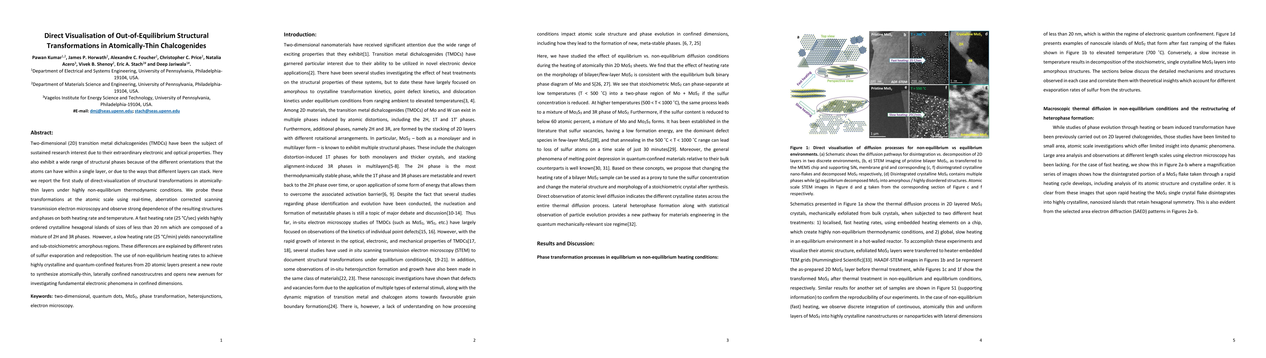
Papers on arXiv
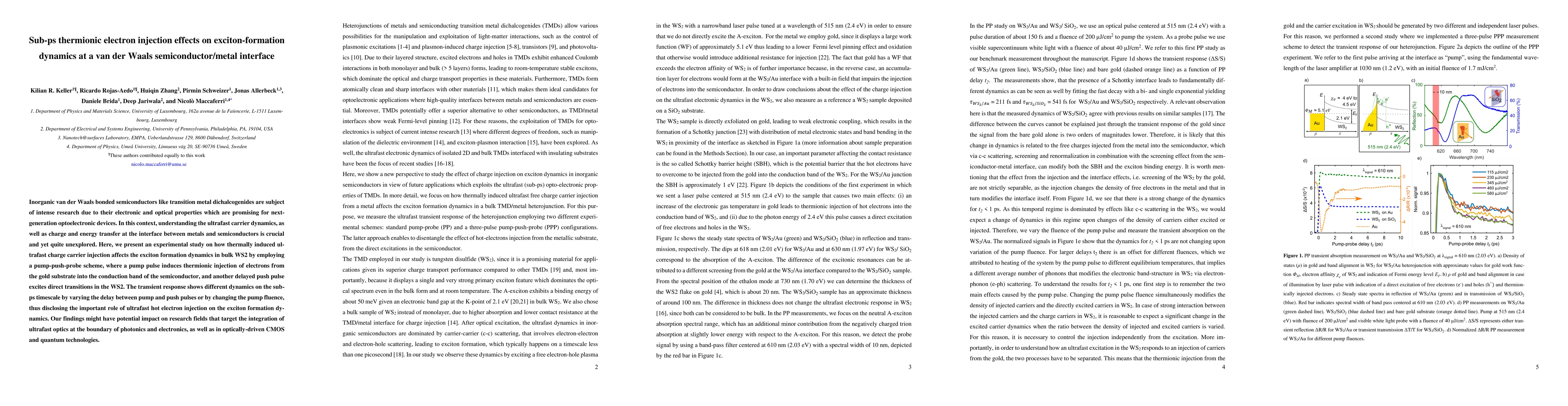
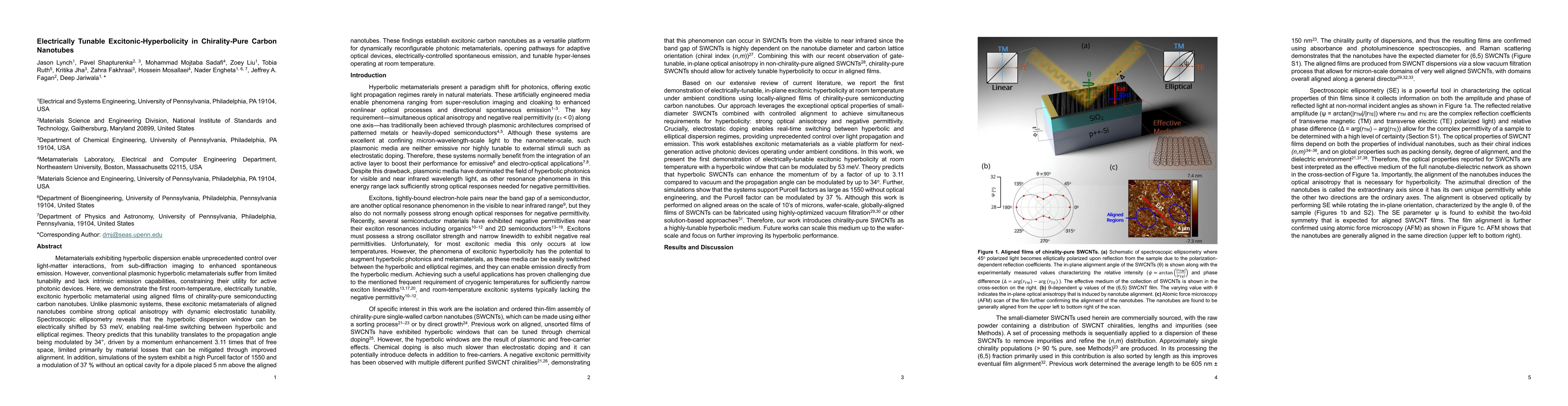
Excitonic semiconductors are attractive for next-generation photovoltaics (PVs) with lower cost, lighter weight, and lower material consumption than conventional technologies. Among them, transition...
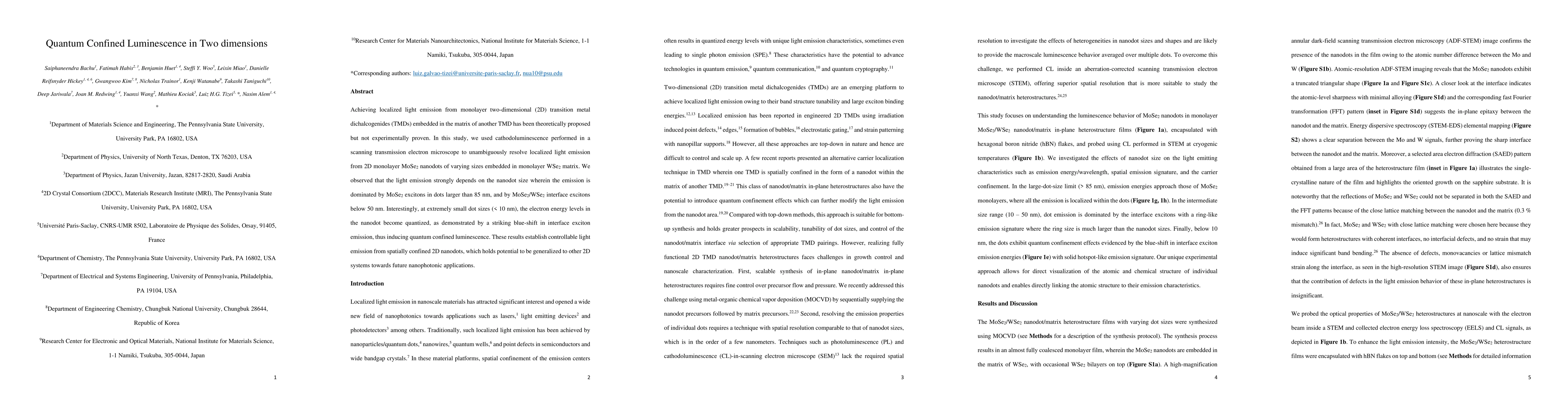
The demand for high-efficiency photovoltaic systems necessitates innovations that transcend the efficiency limitations of single-junction solar cells. This study investigates a tandem photovoltaic a...
Achieving localized light emission from monolayer two-dimensional (2D) transition metal dichalcogenides (TMDs) embedded in the matrix of another TMD has been theoretically proposed but not experimen...
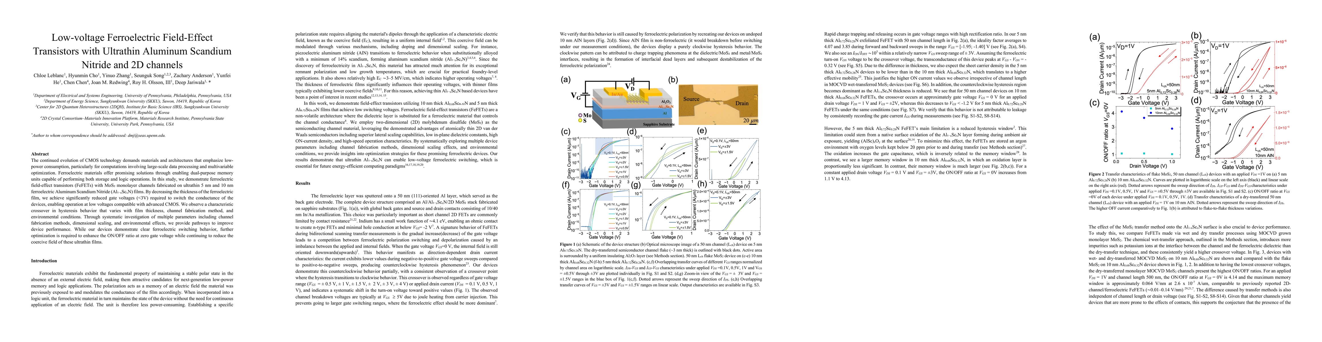
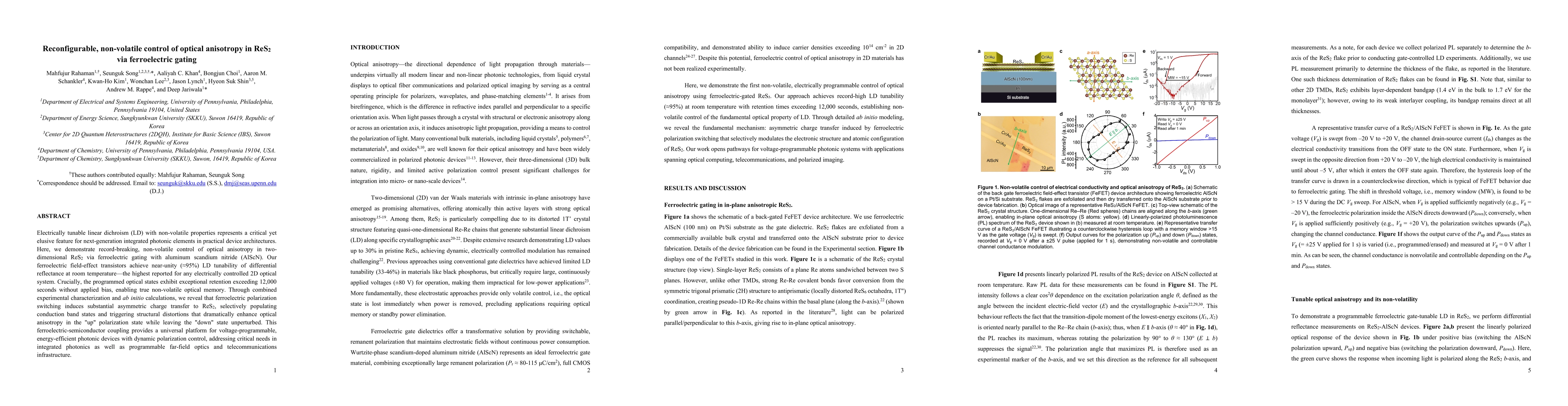
Ferroelectric field-effect transistors (FeFET) with two-dimensional (2D) semiconductor channels are promising low-power, embedded non-volatile memory (NVM) candidates for next-generation in-memory c...
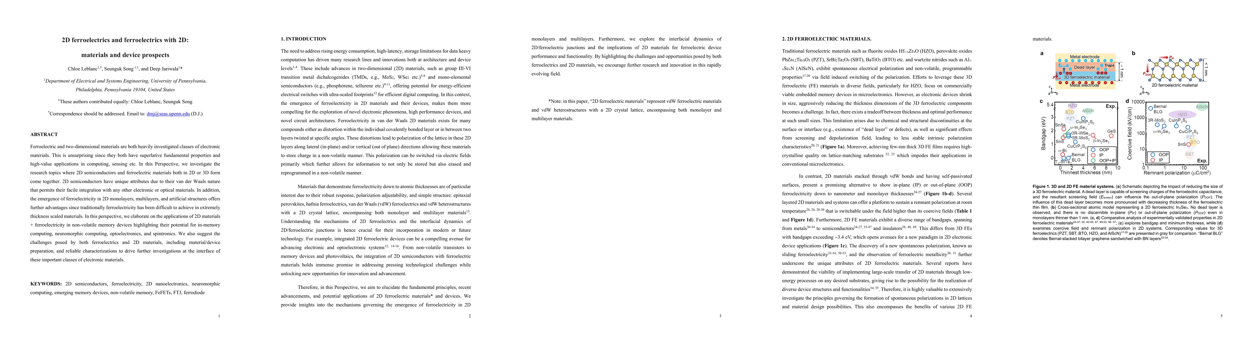
Ferroelectric and two-dimensional materials are both heavily investigated classes of electronic materials. This is unsurprising since they both have superlative fundamental properties and high-value...
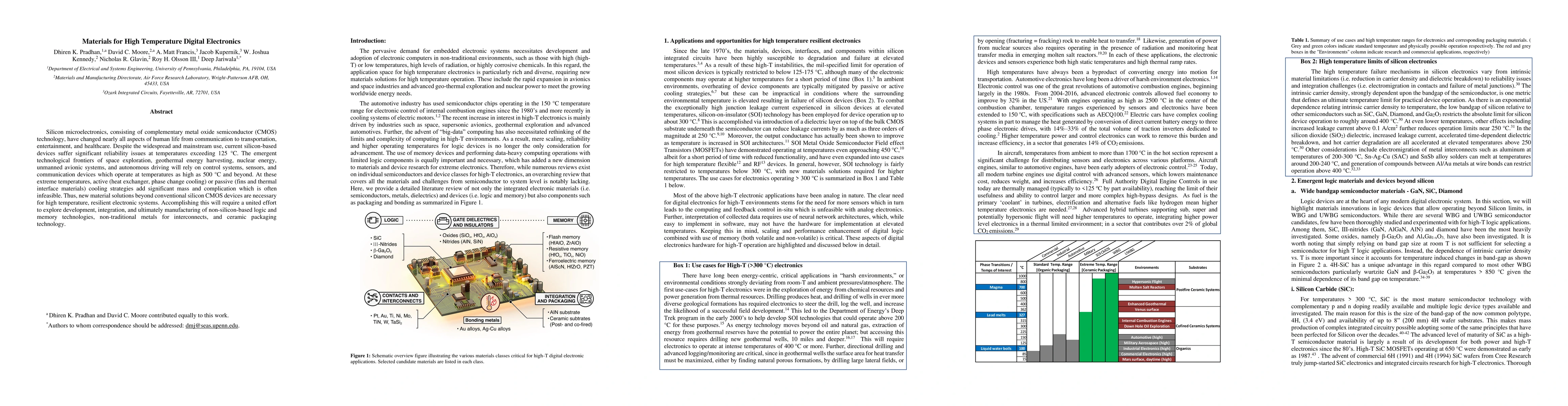
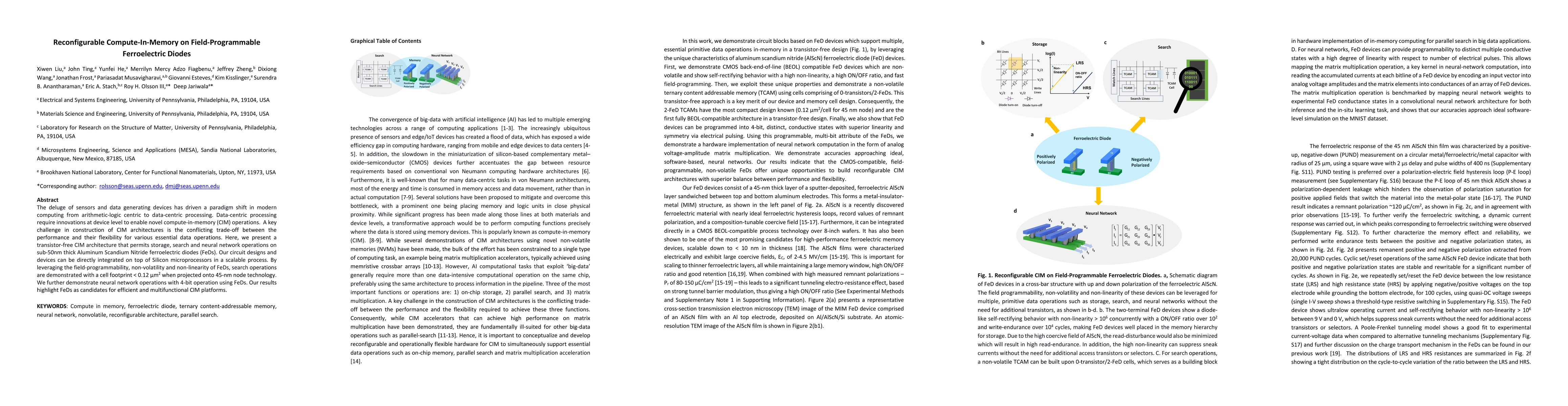
Silicon microelectronics, consisting of complementary metal oxide semiconductor (CMOS) technology, have changed nearly all aspects of human life from communication to transportation, entertainment, ...
The growth in data generation necessitates efficient data processing technologies to address the von Neumann bottleneck in conventional computer architecture. Memory-driven computing, which integrat...
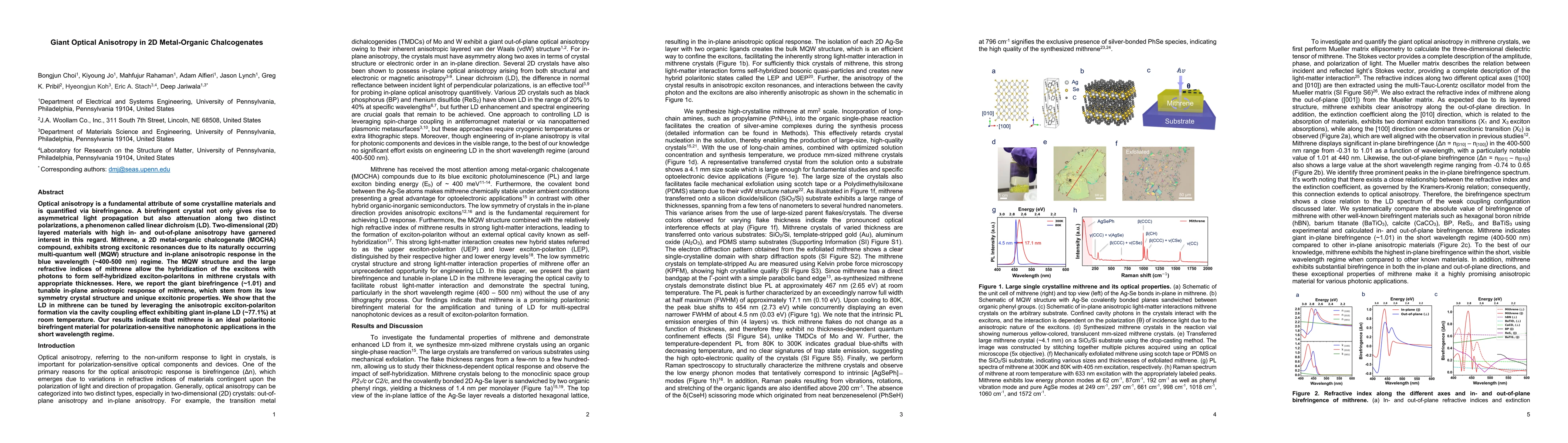
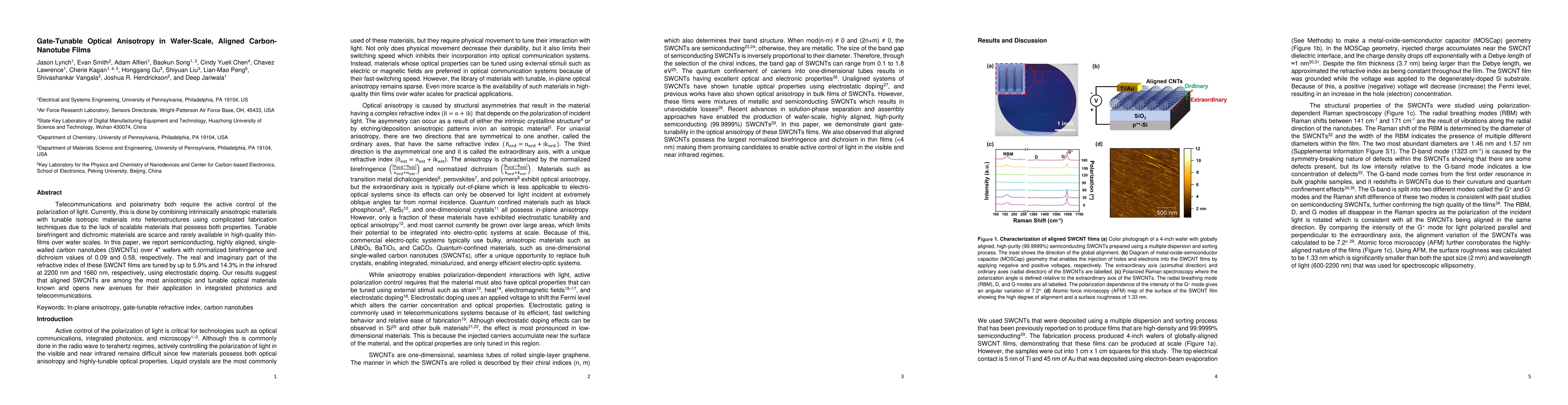
Optical anisotropy is a fundamental attribute of some crystalline materials and is quantified via birefringence. A birefringent crystal not only gives rise to asymmetrical light propagation but also...
Surface Acoustic Wave (SAW) devices featuring Aluminum Scandium Nitride (AlScN) on a 4H-Silicon Carbide (SiC) substrate, offer a unique blend of high sound velocity, low thermal resistance, substant...
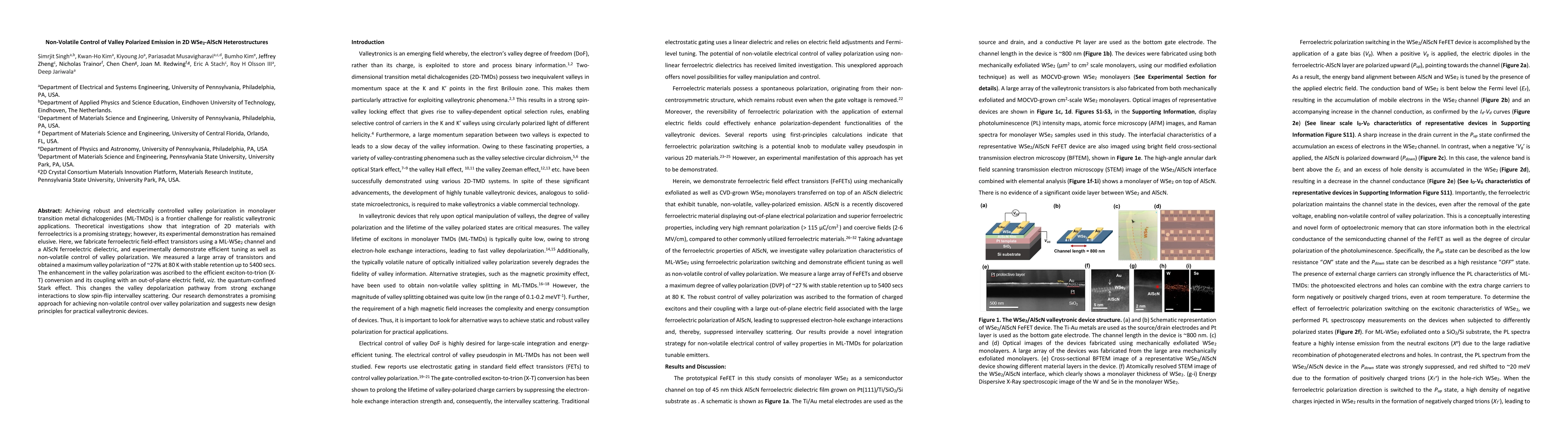
Achieving robust and electrically controlled valley polarization in monolayer transition metal dichalcogenides (ML-TMDs) is a frontier challenge for realistic valleytronic applications. Theoretical ...
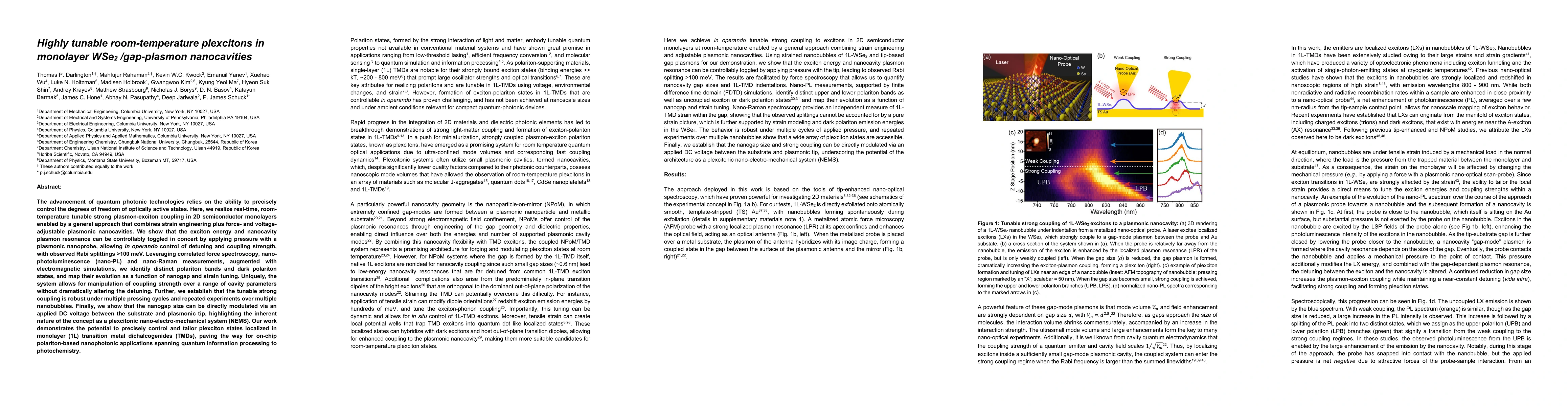
The advancement of quantum photonic technologies relies on the ability to precisely control the degrees of freedom of optically active states. Here, we realize real-time, room-temperature tunable st...
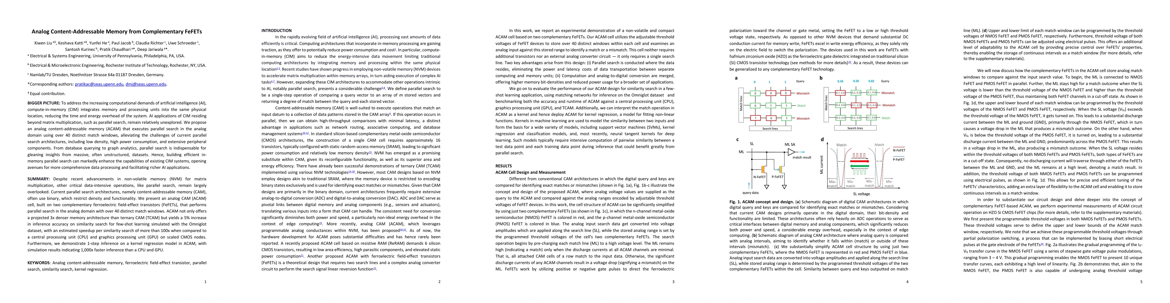
To address the increasing computational demands of artificial intelligence (AI) and big data, compute-in-memory (CIM) integrates memory and processing units into the same physical location, reducing...
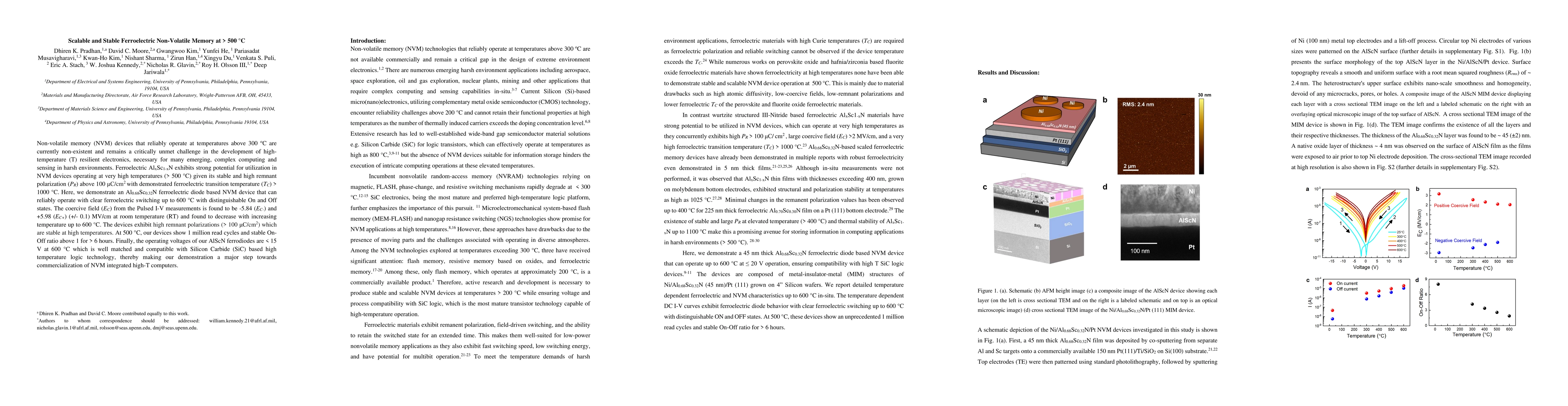
Non-volatile memory (NVM) devices that reliably operate at temperatures above 300 $^\circ$C are currently non-existent and remains a critically unmet challenge in the development of high-temperature...
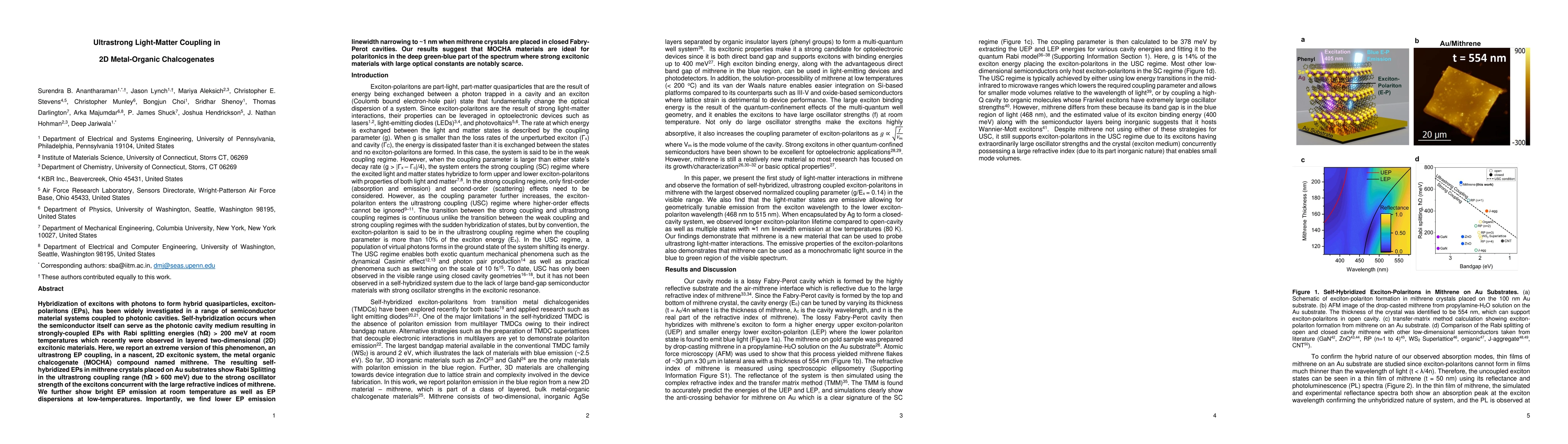
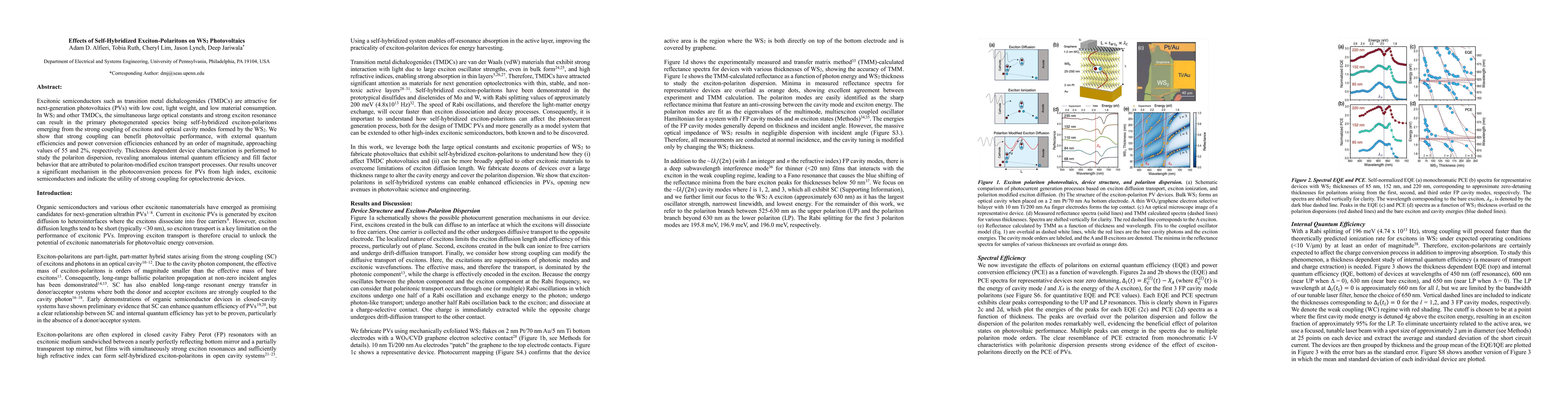
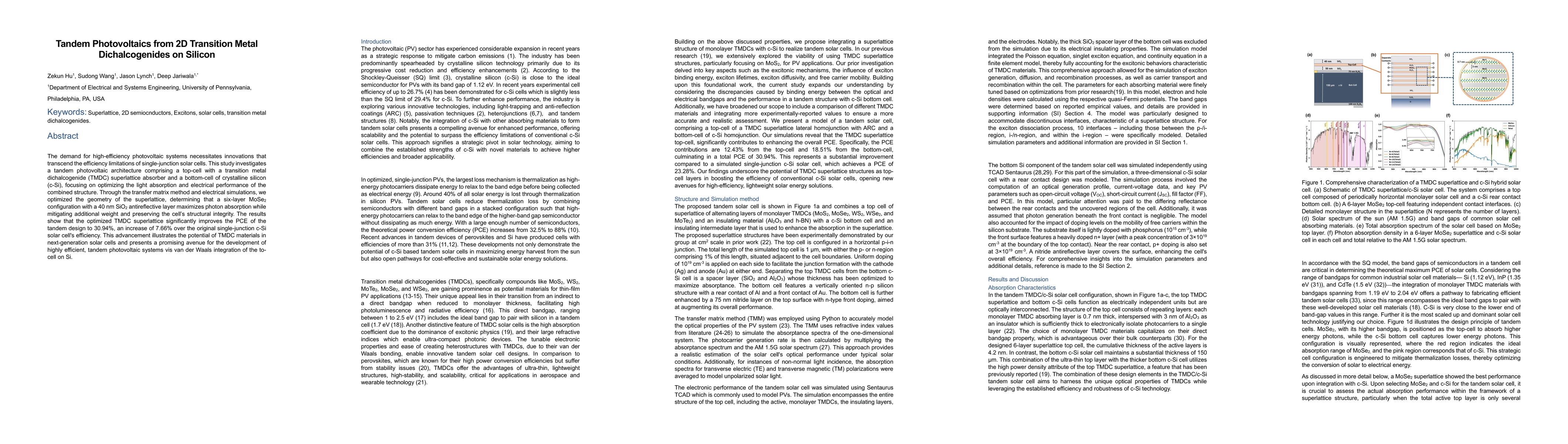
Hybridization of excitons with photons to form hybrid quasiparticles, exciton-polaritons (EPs), has been widely investigated in a range of semiconductor material systems coupled to photonic cavities...
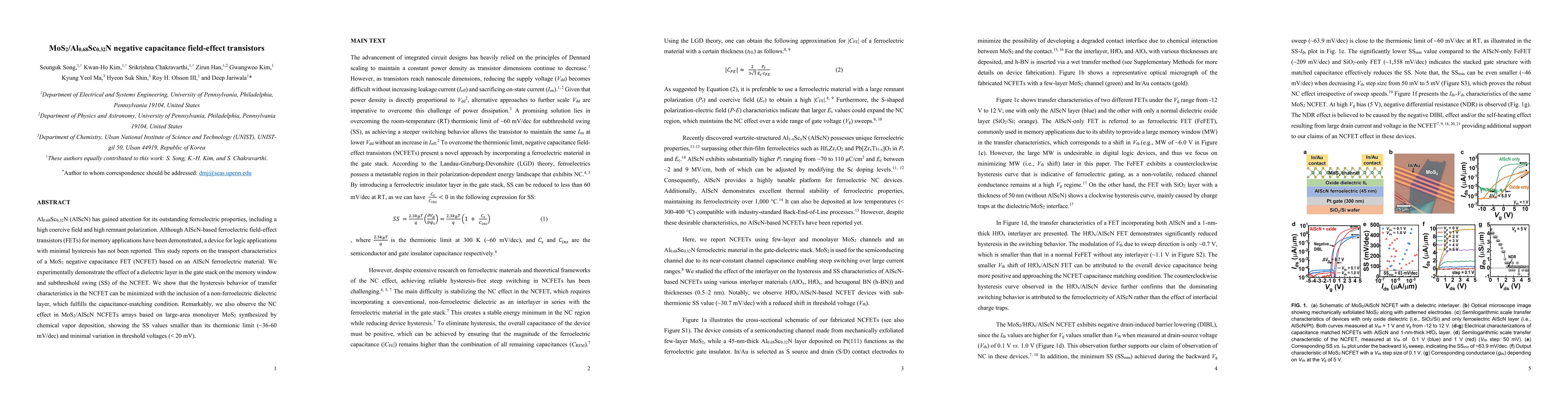
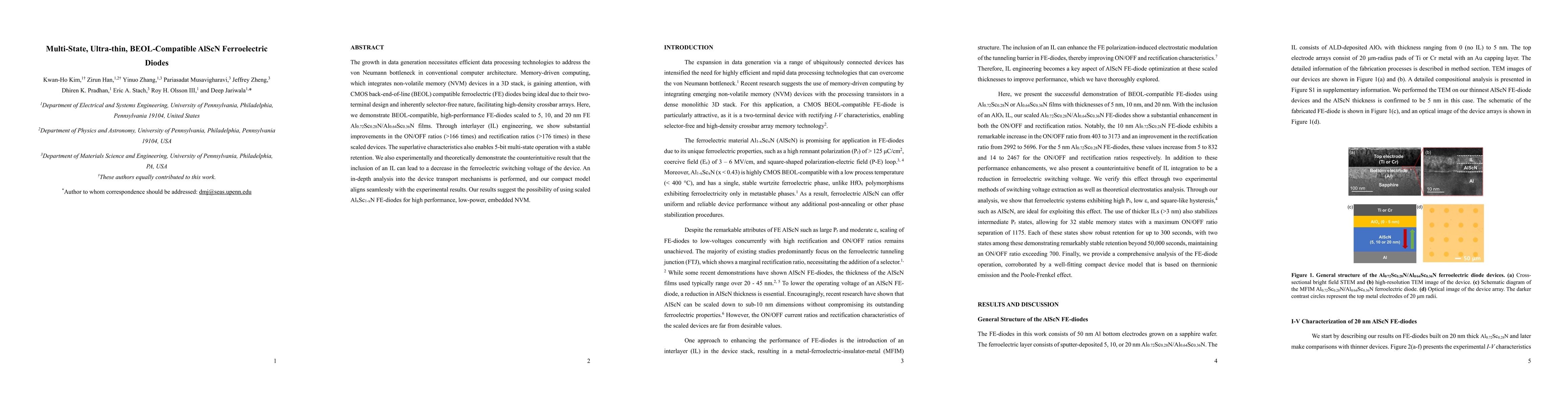
Al$_{0.68}$Sc$_{0.32}$N (AlScN) has gained attention for its outstanding ferroelectric properties, including a high coercive field and high remnant polarization. Although AlScN-based ferroelectric f...
Two-dimensional (2D) semiconductors are promising candidates for optoelectronic application and quantum information processes due to their inherent out-of-plane 2D confinement. In addition, they off...
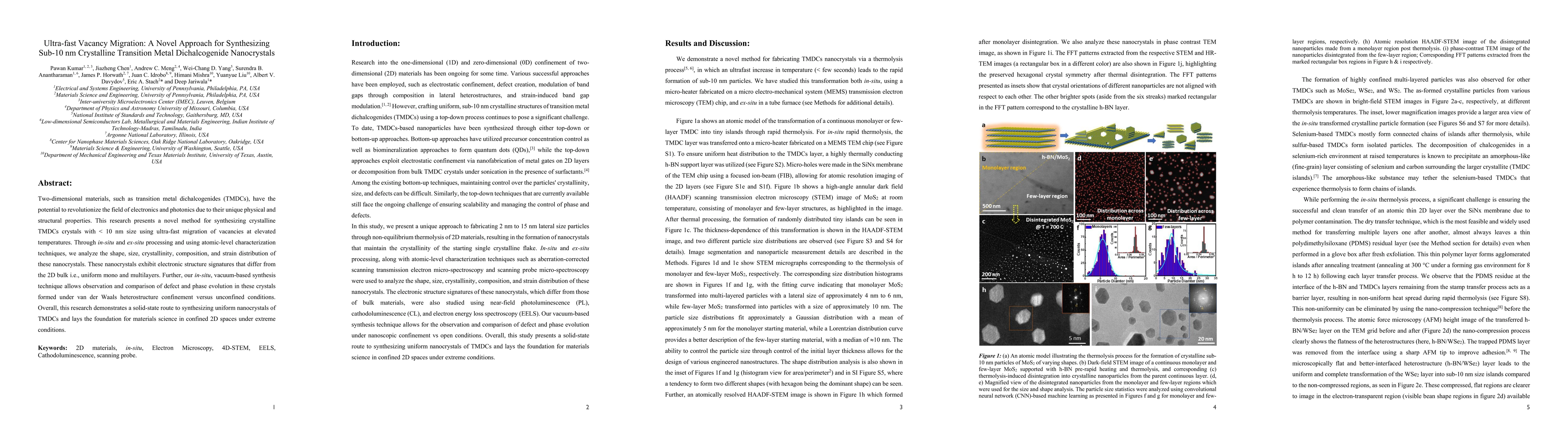
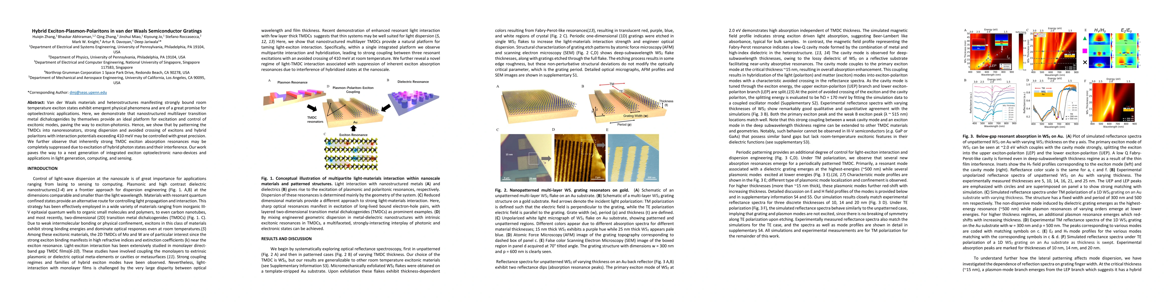
Two-dimensional materials, such as transition metal dichalcogenides (TMDCs), have the potential to revolutionize the field of electronics and photonics due to their unique physical and structural pr...
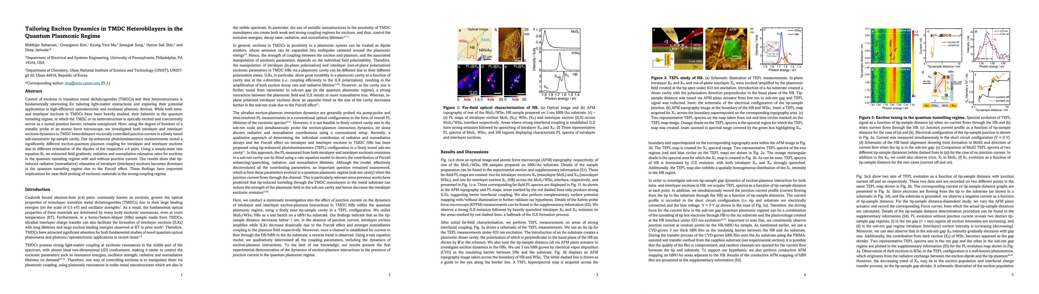
Control of excitons in transition metal dichalcogenides (TMDCs) and their heterostructures is fundamentally interesting for tailoring light-matter interactions and exploring their potential applicat...
Telecommunications and polarimetry both require the active control of the polarization of light, Currently, this is done by combining intrinsically anisotropic materials with tunable isotropic mater...
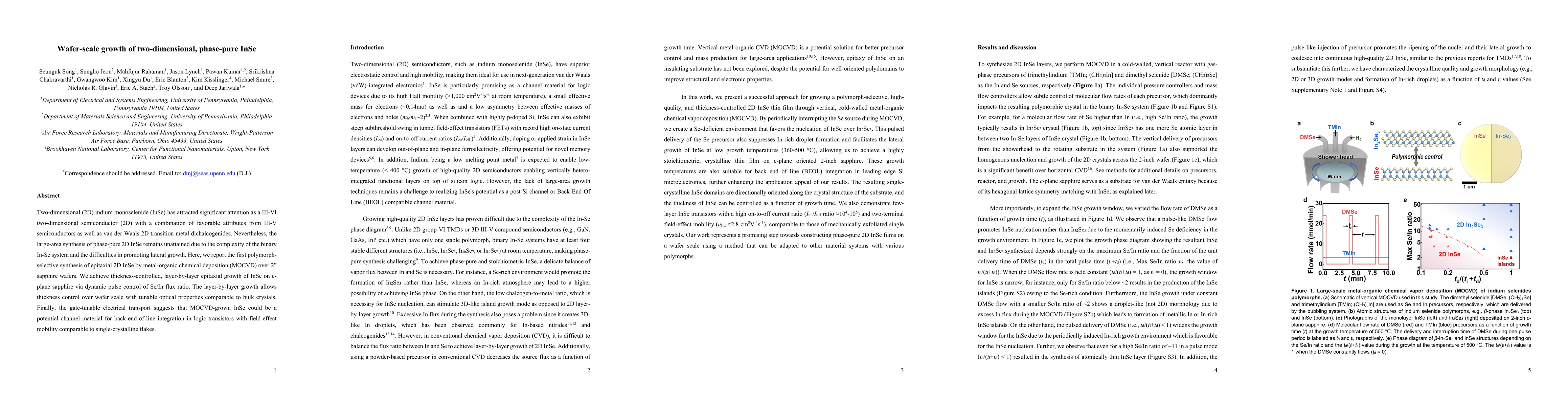
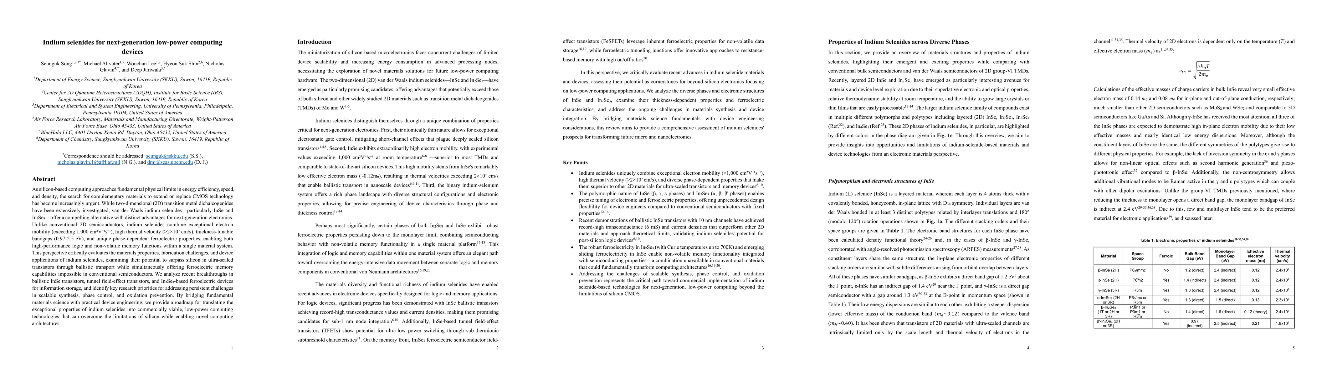
Two-dimensional (2D) indium monoselenide (InSe) has attracted significant attention as a III-VI two-dimensional semiconductor (2D) with a combination of favorable attributes from III-V semiconductor...
Excitons, bound electron-hole pairs, in Two-Dimensional Hybrid Organic Inorganic Perovskites (2D HOIPs) are capable of forming hybrid light-matter states known as exciton-polaritons (E-Ps) when the ...
Excitonic semiconductors have been a subject of research for photovoltaic applications for many decades. Among them, the organic polymers and small molecules based solar cells have now exceeded 19% ...
Compact electro-optic (EO) modulators with large extinction ratios, low-switching energies, and high operation speeds are desirable for integrated photonic and linear optical computing. Traditional ...
Two-dimensional (2D) materials present an exciting opportunity for devices and systems beyond the von Neumann computing architecture paradigm due to their diversity of electronic structure, physical...
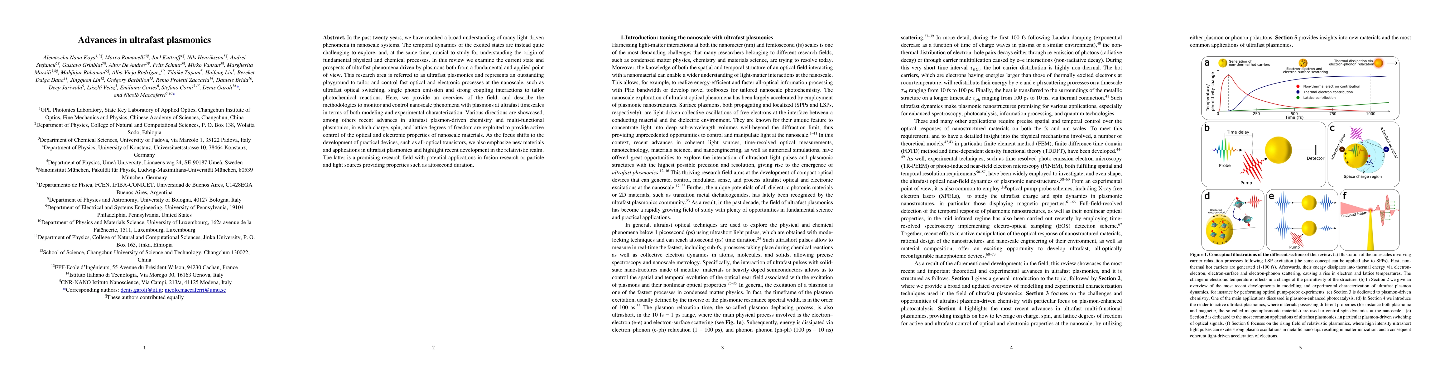
In the past twenty years, we have reached a broad understanding of many light-driven phenomena in nanoscale systems. The temporal dynamics of the excited states are instead quite challenging to expl...
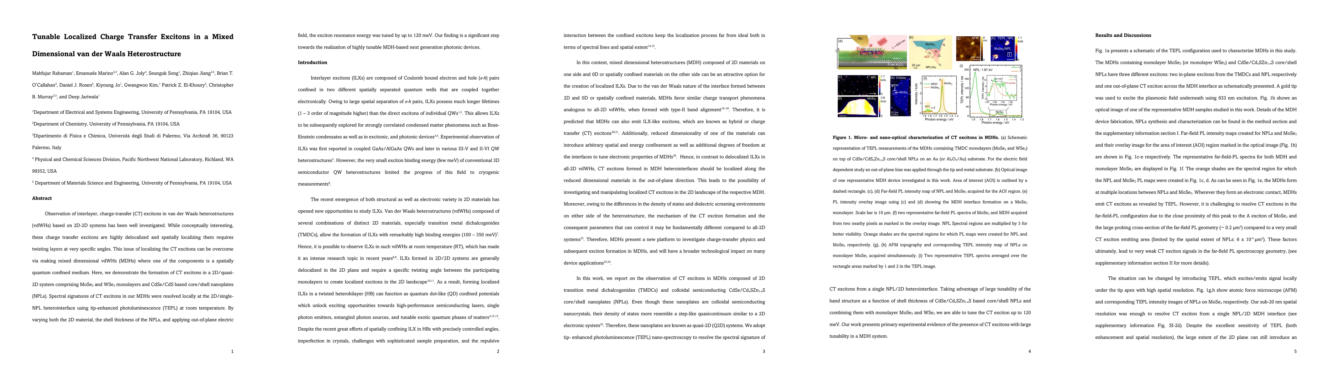
Observation of interlayer, charge-transfer (CT) excitons in van der Waals heterostructures (vdWHs) based on 2D-2D systems has been well investigated. While conceptually interesting, these charge tra...
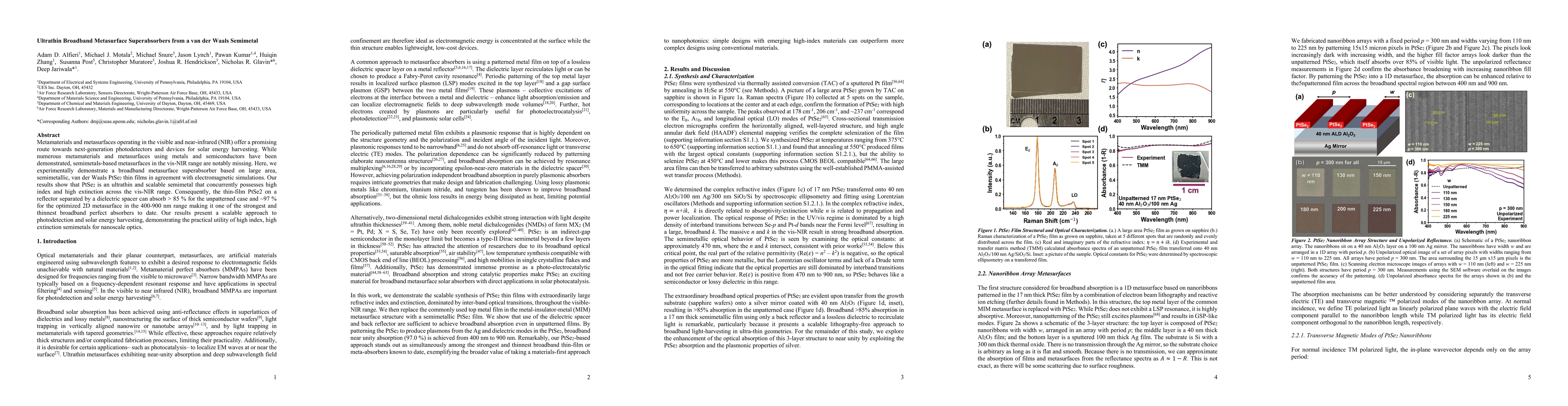
Metamaterials and metasurfaces operating in the visible and near-infrared (NIR) offer a promising route towards next-generation photodetectors and devices for solar energy harvesting. While numerous...
Strong light-matter interactions in localized nano-emitters when placed near metallic mirrors have been widely reported via spectroscopic studies in the optical far-field. Here, we report a near-fie...
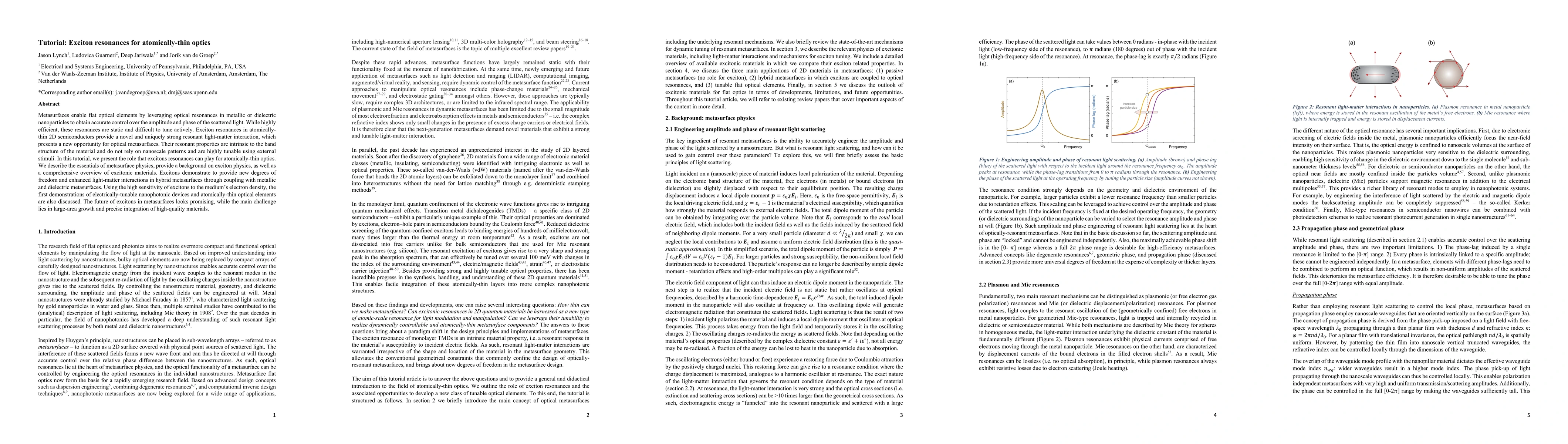
Metasurfaces enable flat optical elements by leveraging optical resonances in metallic or dielectric nanoparticles to obtain accurate control over the amplitude and phase of the scattered light. Whi...
Two-dimensional (2D) magnetic van der Waals materials provide a powerful platform for studying fundamental physics of low-dimensional magnetism, engineering novel magnetic phases, and enabling ultra...
Two-dimensional chalcogenide semiconductors have recently emerged as a host material for quantum emitters of single photons. While several reports on defect and strain-induced single photon emission...
Two-dimensional (2D) hybrid organic-inorganic perovskites (HOIPs) are promising candidates for optoelectronic applications due to their efficient light emission properties, and strong dielectric con...
The deluge of sensors and data generating devices has driven a paradigm shift in modern computing from arithmetic-logic centric to data centric processing. At a hardware level, this presents an urge...
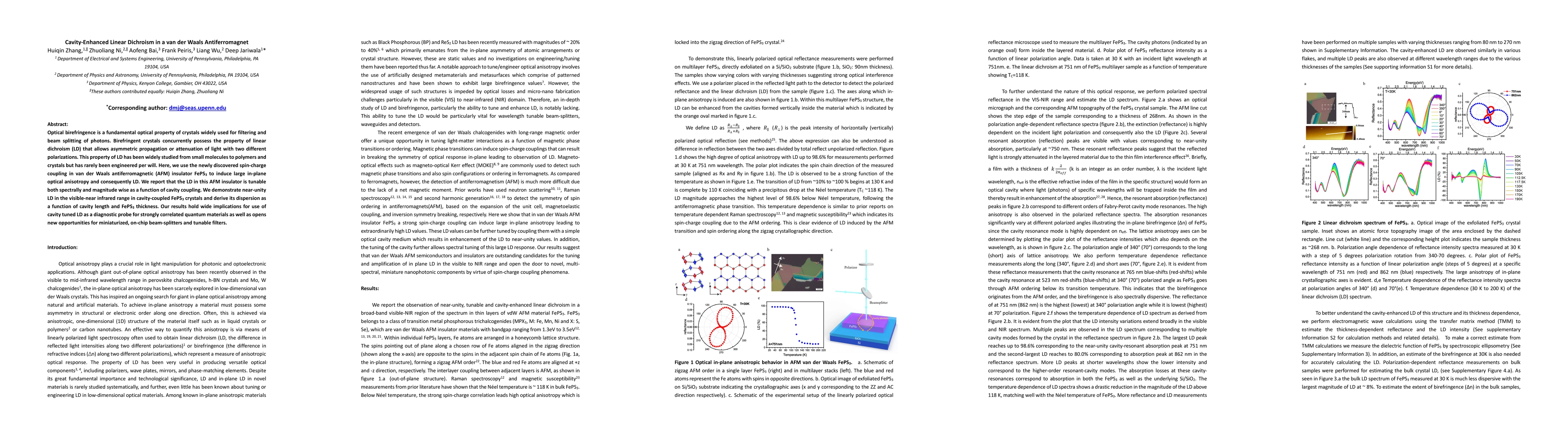
Optical birefringence is a fundamental optical property of crystals widely used for filtering and beam splitting of photons. Birefringent crystals concurrently possess the property of linear dichroi...
Inorganic van der Waals bonded semiconductors like transition metal dichalcogenides are subject of intense research due to their electronic and optical properties which are promising for next-genera...
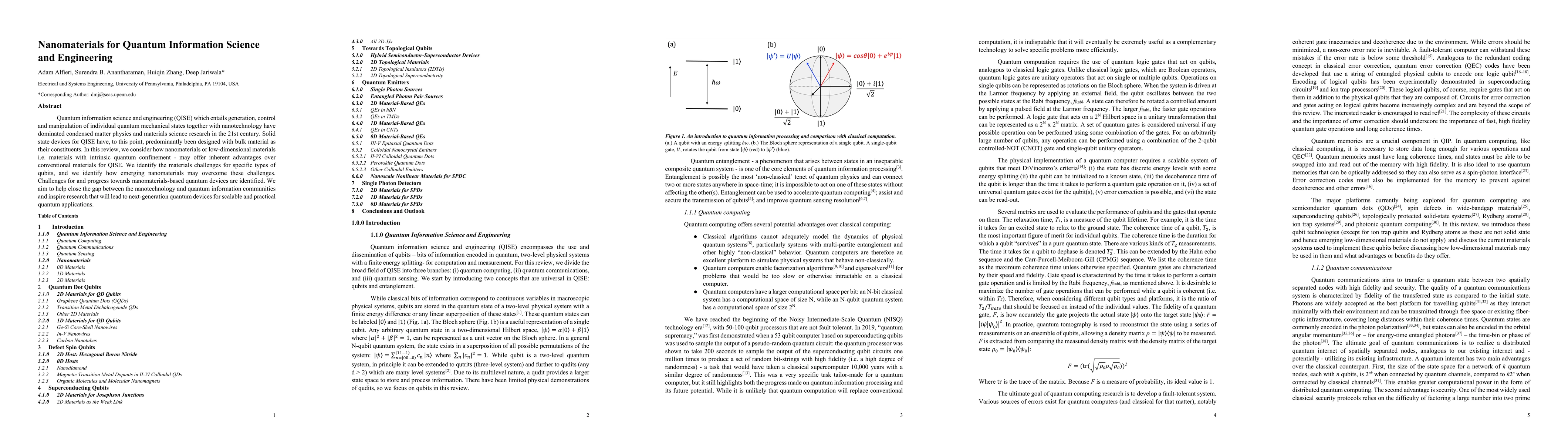
Quantum information science and engineering (QISE) which entails use of quantum mechanical states for information processing, communications, and sensing and the area of nanoscience and nanotechnolo...
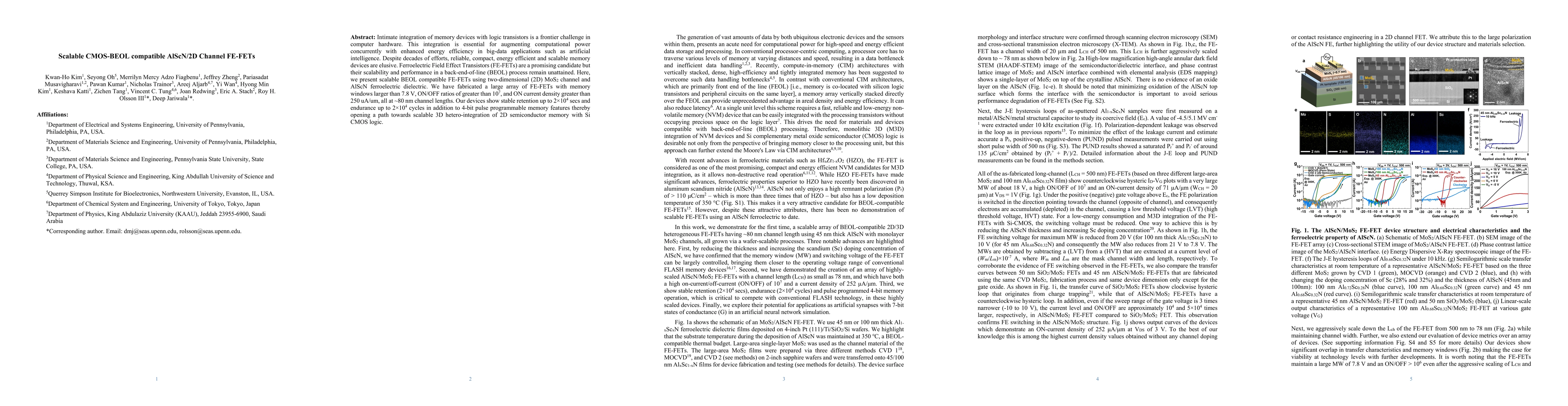
Intimate integration of memory devices with logic transistors is a frontier challenge in computer hardware. This integration is essential for augmenting computational power concurrently with enhance...
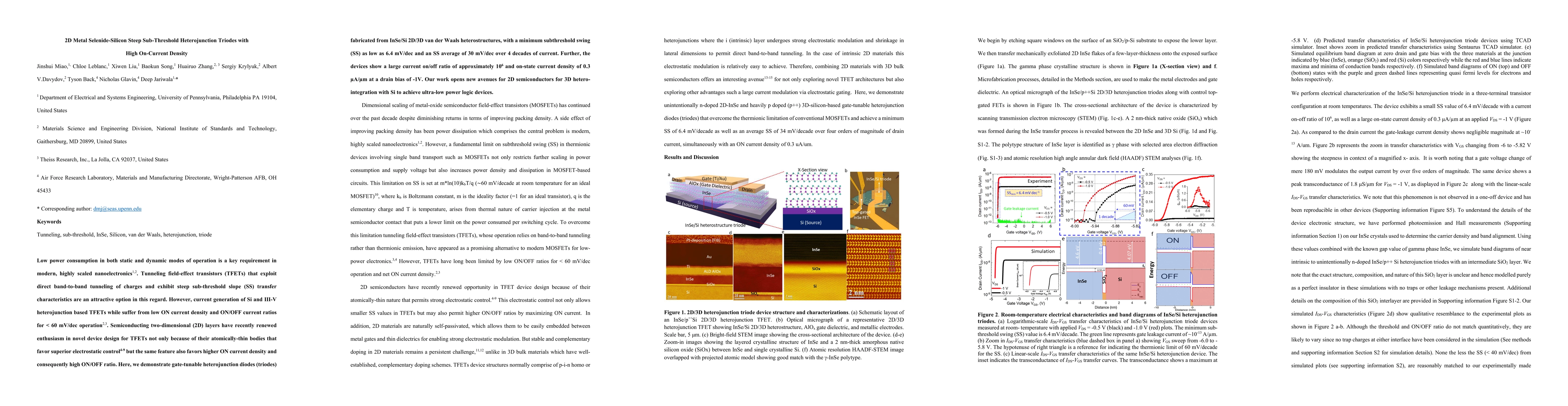
Low power consumption in both static and dynamic modes of operation is a key requirement in modern, highly scaled nanoelectronics. Tunneling field-effect transistors (TFETs) that exploit direct band...
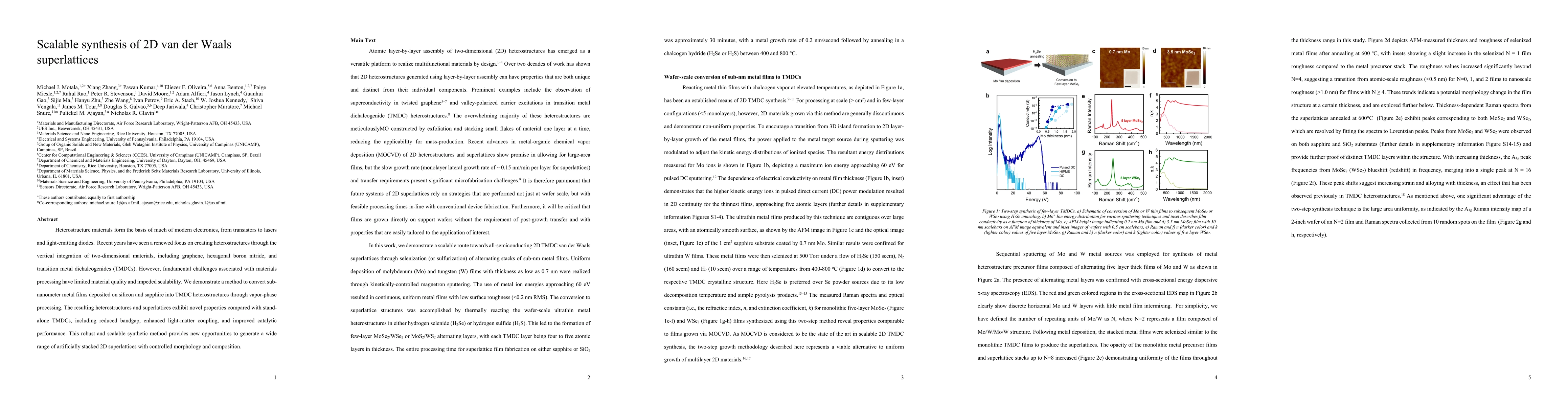
Heterostructure materials form the basis of much of modern electronics, from transistors to lasers and light-emitting diodes. Recent years have seen a renewed focus on creating heterostructures thro...
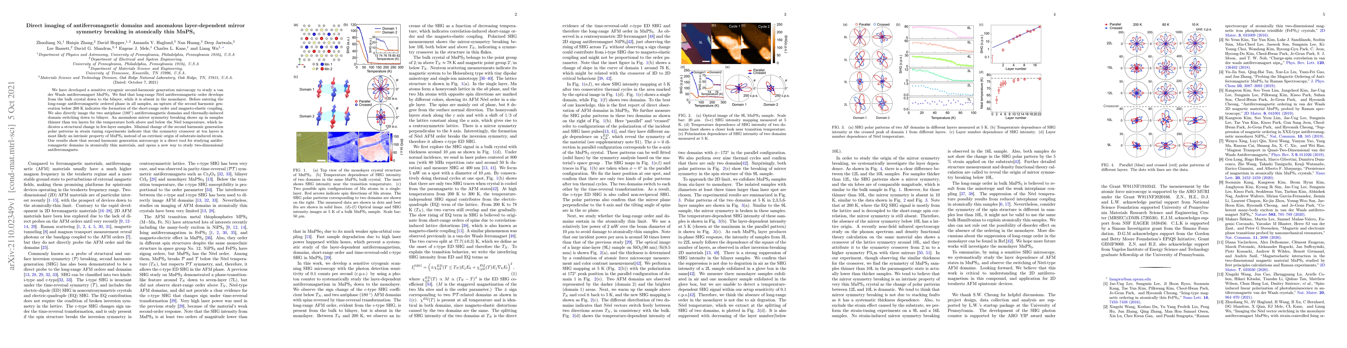
We have developed a sensitive cryogenic second-harmonic generation microscopy to study a van der Waals antiferromagnet MnPS$_3$. We find that long-range N\'eel antiferromagnetic order develops from ...
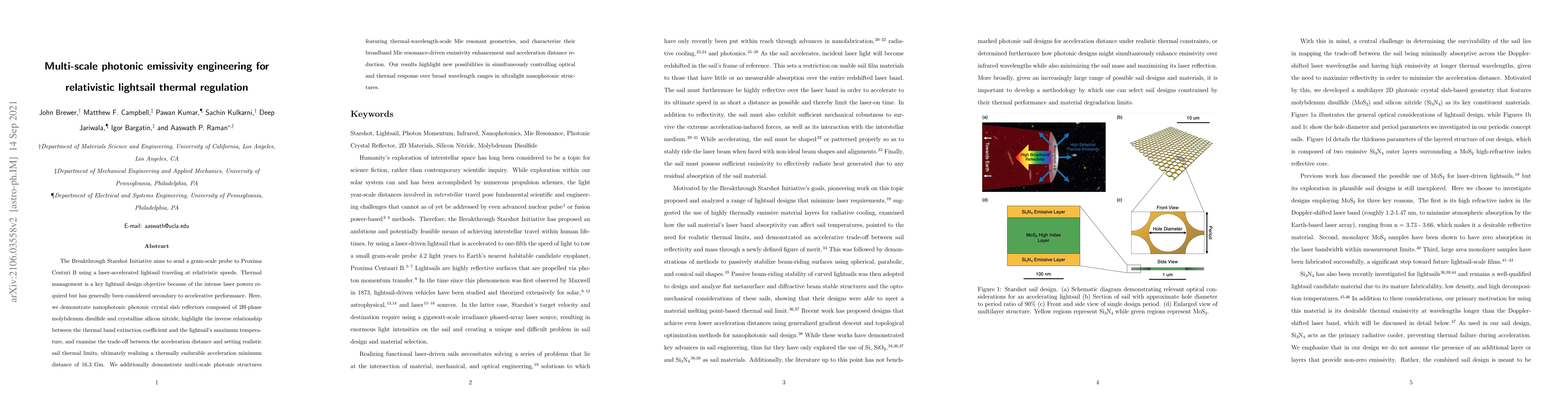
The Breakthrough Starshot Initiative aims to send a gram-scale probe to Proxima Centuri B using a laser-accelerated lightsail traveling at relativistic speeds. Thermal management is a key lightsail ...
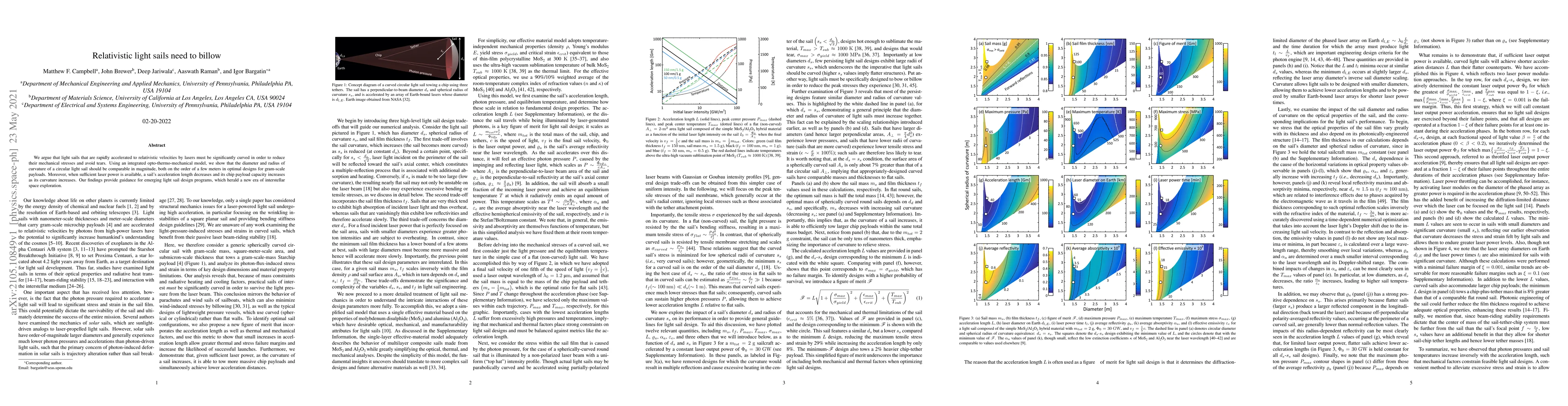
We argue that light sails that are rapidly accelerated to relativistic velocities by lasers must be significantly curved in order to reduce their mechanical stresses and avoid tears. Using an integr...
Light-matter coupling in excitonic materials has been the subject of intense investigation due to emergence of new excitonic materials. Two-dimensional layered hybrid organic/inorganic perovskites (...
The interest in two-dimensional and layered materials continues to expand, driven by the compelling properties of individual atomic layers that can be stacked and/or twisted into synthetic heterostr...
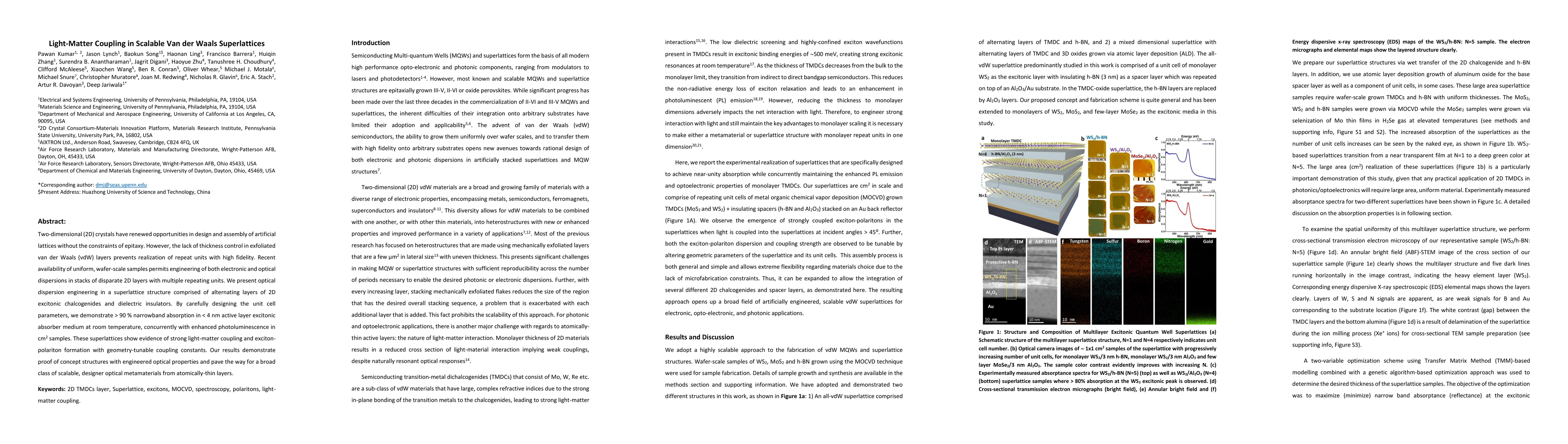
Two-dimensional (2D) crystals have renewed opportunities in design and assembly of artificial lattices without the constraints of epitaxy. However, the lack of thickness control in exfoliated van de...
Van der Waals materials exhibit naturally passivated surfaces and can form versatile heterostructures, enabling observation of carrier transport mechanisms not seen in three-dimensional materials. H...
Semiconductors in all dimensionalities ranging from 0D quantum dots and molecules to 3D bulk crystals support bound electron-hole pair quasiparticles termed as excitons. Over the past two decades, t...
The semiconductor-metal junction is one of the most critical factors for high performance electronic devices. In two-dimensional (2D) semiconductor devices, minimizing the voltage drop at this junct...
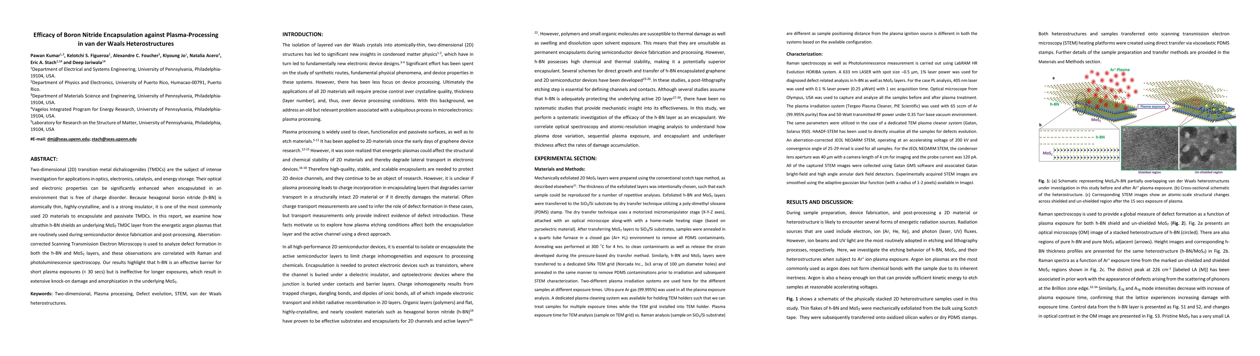
Two-dimensional (2D) transition metal dichalcogenides (TMDCs) are the subject of intense investigation for applications in optics, electronics, catalysis, and energy storage. Their optical and elect...
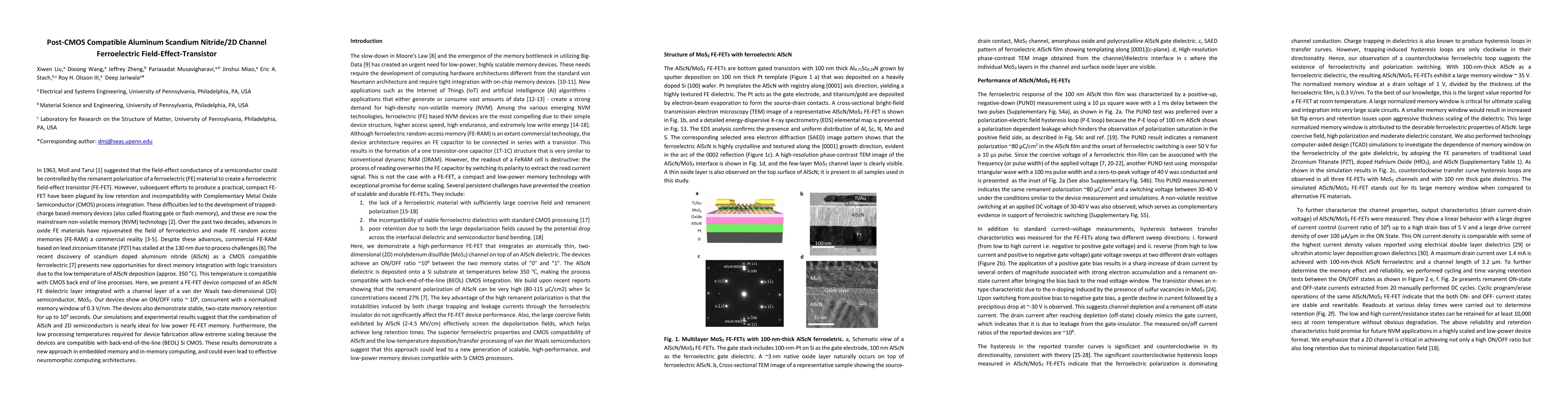
In 1963, Moll and Tarui suggested that the field-effect conductance of a semiconductor could be controlled by the remanent polarization of a ferroelectric (FE) material to create a ferroelectric fie...
Two-dimensional (2D) hybrid organic inorganic perovskite (HOIP) semiconductors have attracted widespread attention as a platform of next generation optoelectronic devices benefiting from their natur...
Electrically-tunable optical properties in materials are desirable for many applications ranging from displays to lasing and optical communication. In most two-dimensional thin-films and other quant...
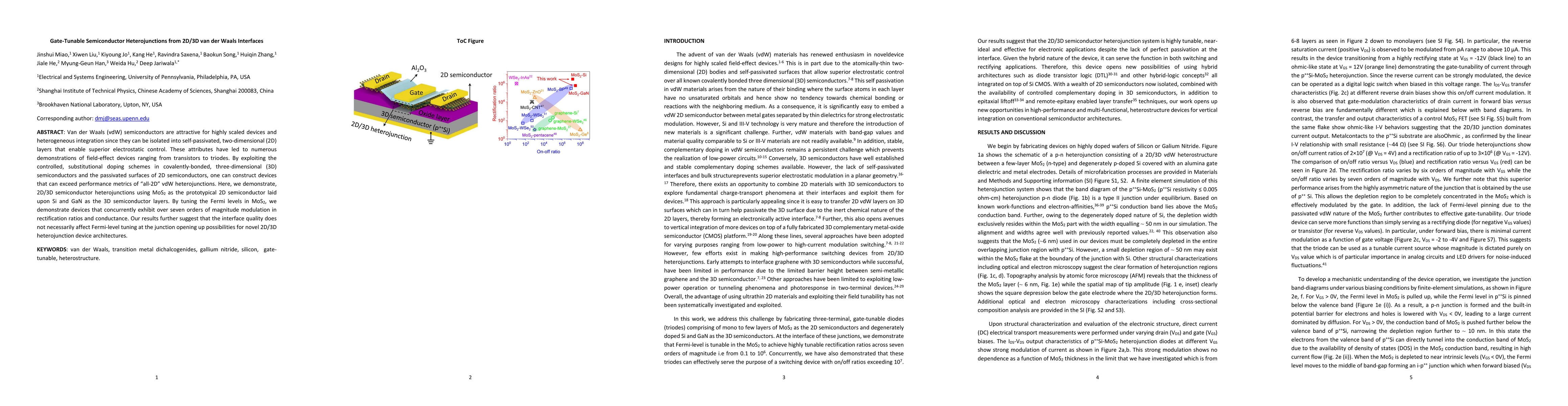
Van der Waals (vdW) semiconductors are attractive for highly scaled devices and heterogeneous integration since they can be isolated into self-passivated, two-dimensional (2D) layers that enable sup...
Two-dimensional (2D) transition metal dichalcogenides (TMDCs) have been the subject of sustained research interest due to their extraordinary electronic and optical properties. They also exhibit a w...
Van der Waals materials and heterostructures manifesting strongly bound room temperature exciton states exhibit emergent physical phenomena and are of a great promise for optoelectronic applications...
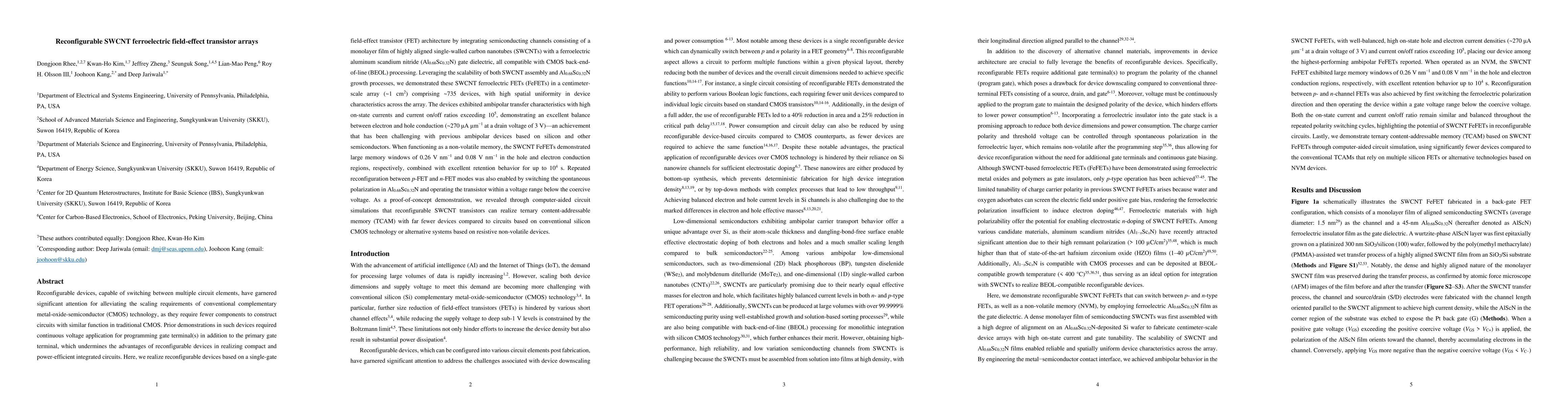
Reconfigurable devices have garnered significant attention for alleviating the scaling requirements of conventional CMOS technology, as they require fewer components to construct circuits with similar...
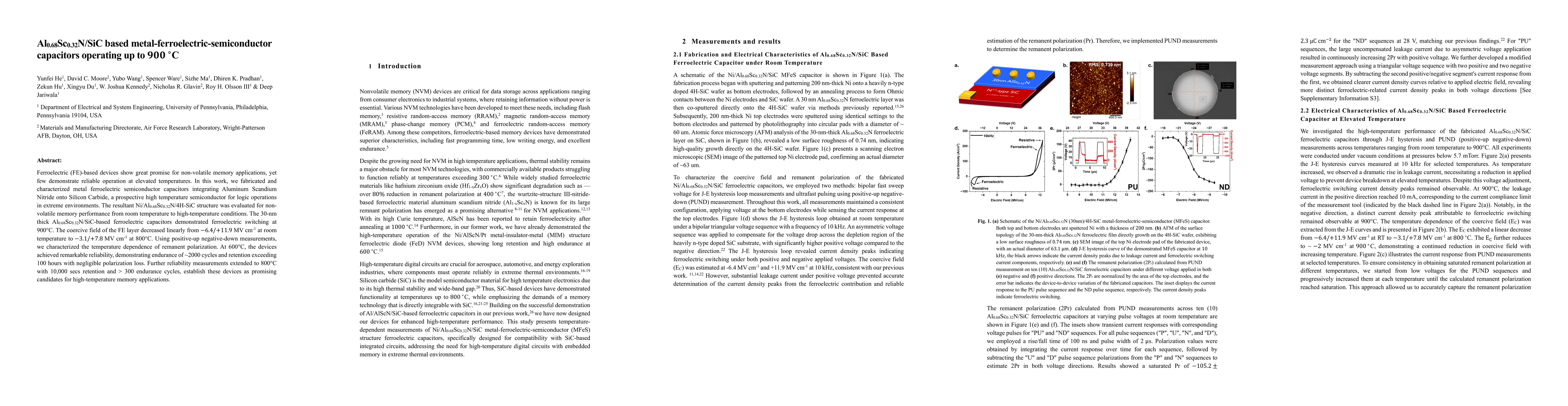
Ferroelectric (FE)-based devices show great promise for non-volatile memory applications, yet few demonstrate reliable operation at elevated temperatures. In this work, we fabricated and characterized...
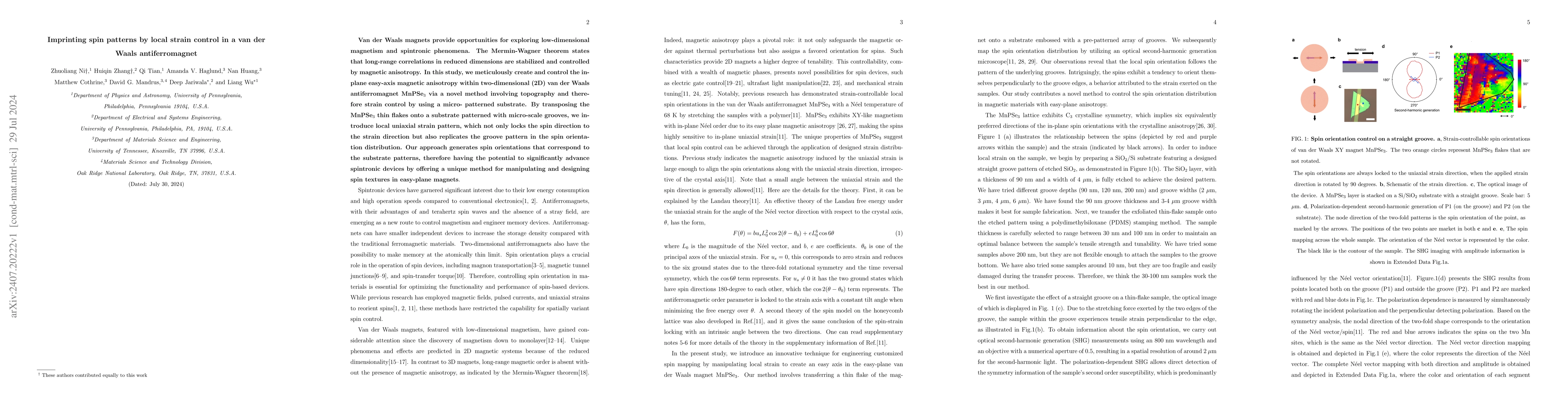
Van der Waals magnets provide opportunities for exploring low-dimensional magnetism and spintronic phenomena. The Mermin-Wagner theorem states that long-range correlations in reduced dimensions are st...
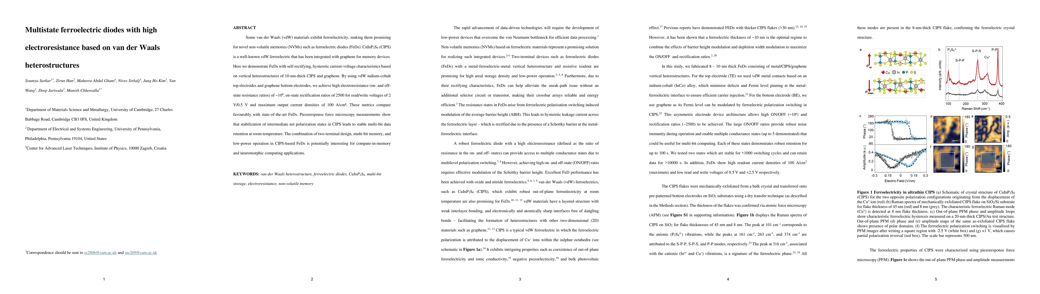
Some van der Waals (vdW) materials exhibit ferroelectricity, making them promising for novel non-volatile memories (NVMs) such as ferroelectric diodes (FeDs). CuInP2S6 (CIPS) is a well-known vdW ferro...
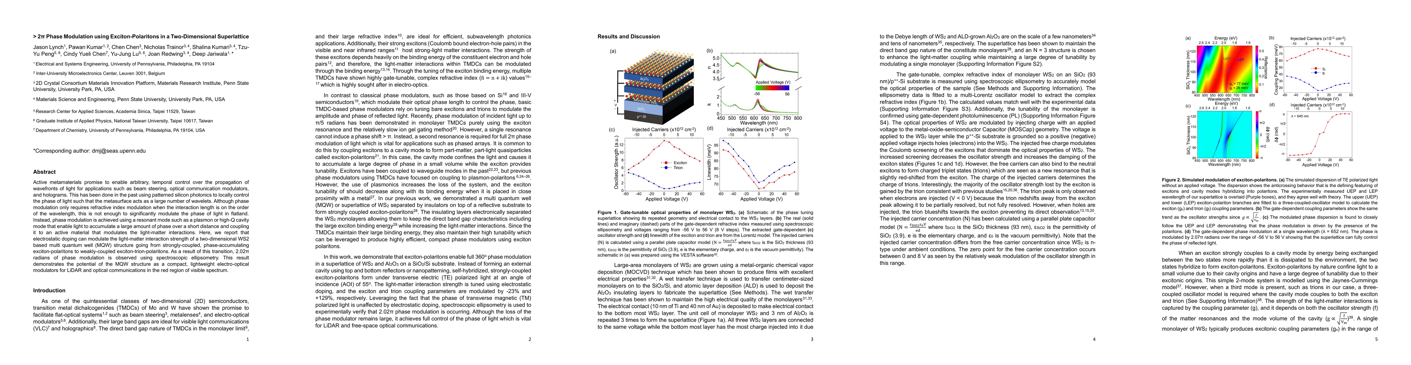
Active metamaterials promise to enable arbitrary, temporal control over the propagation of wavefronts of light for applications such as beam steering, optical communication modulators, and holograms. ...
Broadband absorption in the visible spectrum is essential in optoelectronic applications that involve power conversion such as photovoltaics and photocatalysis. Most ultrathin broadband absorbers use ...
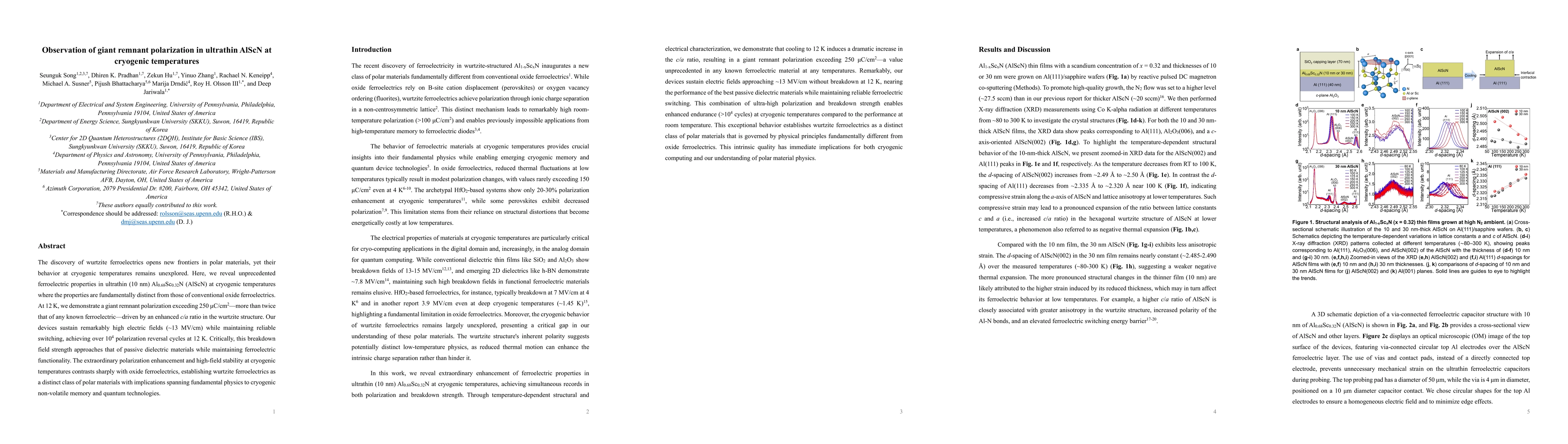
The discovery of wurtzite ferroelectrics opens new frontiers in polar materials, yet their behavior at cryogenic temperatures remains unexplored. Here, we reveal unprecedented ferroelectric properties...
As silicon-based computing approaches fundamental physical limits in energy efficiency, speed, and density, the search for complementary materials to extend or replace CMOS technology has become incre...
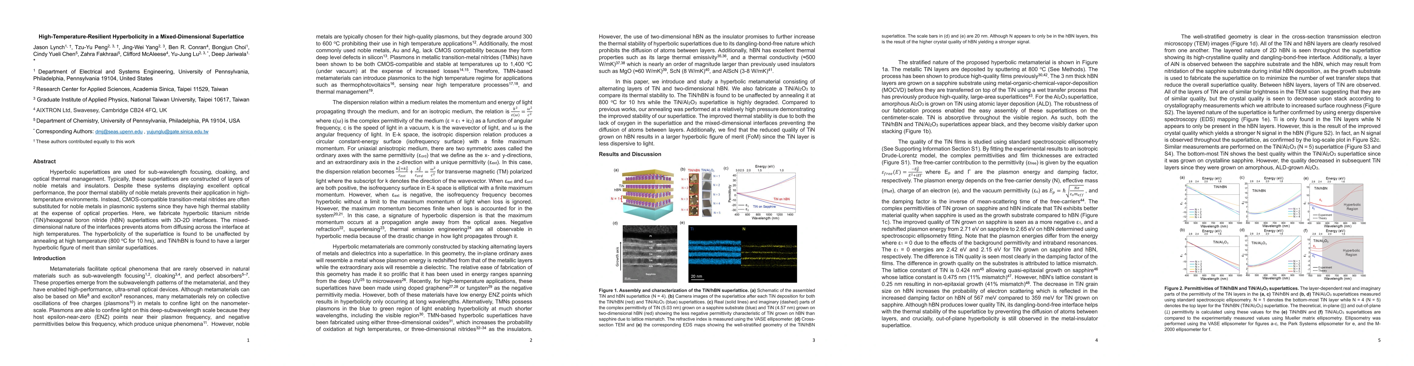
Hyperbolic superlattices are used for sub-wavelength focusing, cloaking, and optical thermal management. Typically, these superlattices are constructed of layers of noble metals and insulators. Despit...
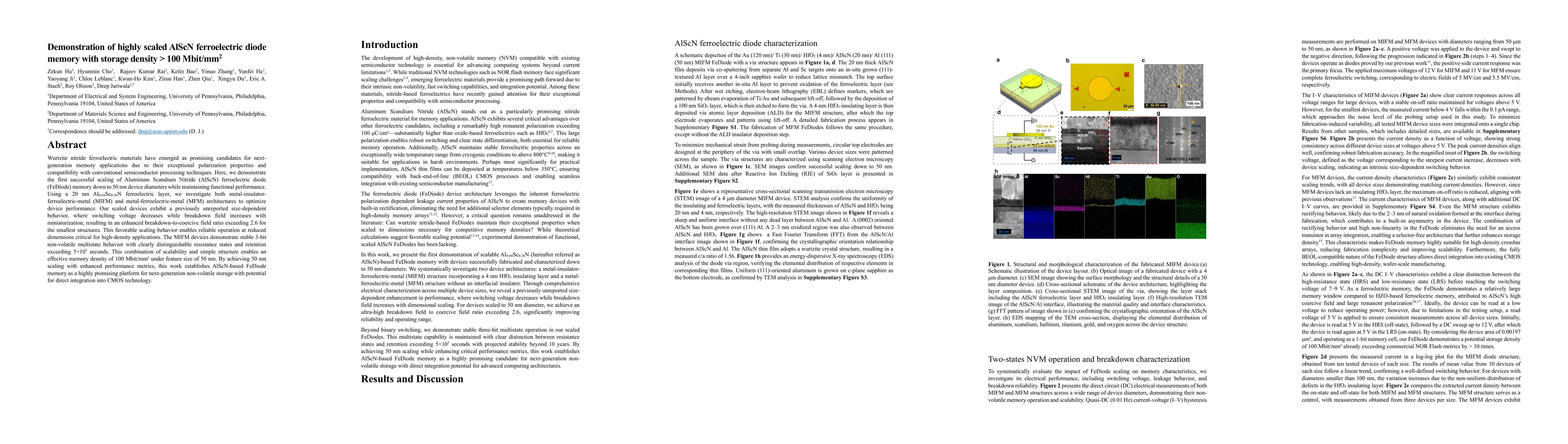
Wurtzite nitride ferroelectric materials have emerged as promising candidates for next-generation memory applications due to their exceptional polarization properties and compatibility with convention...
The continued evolution of CMOS technology demands materials and architectures that emphasize low power consumption, particularly for computations involving large scale data processing and multivariab...
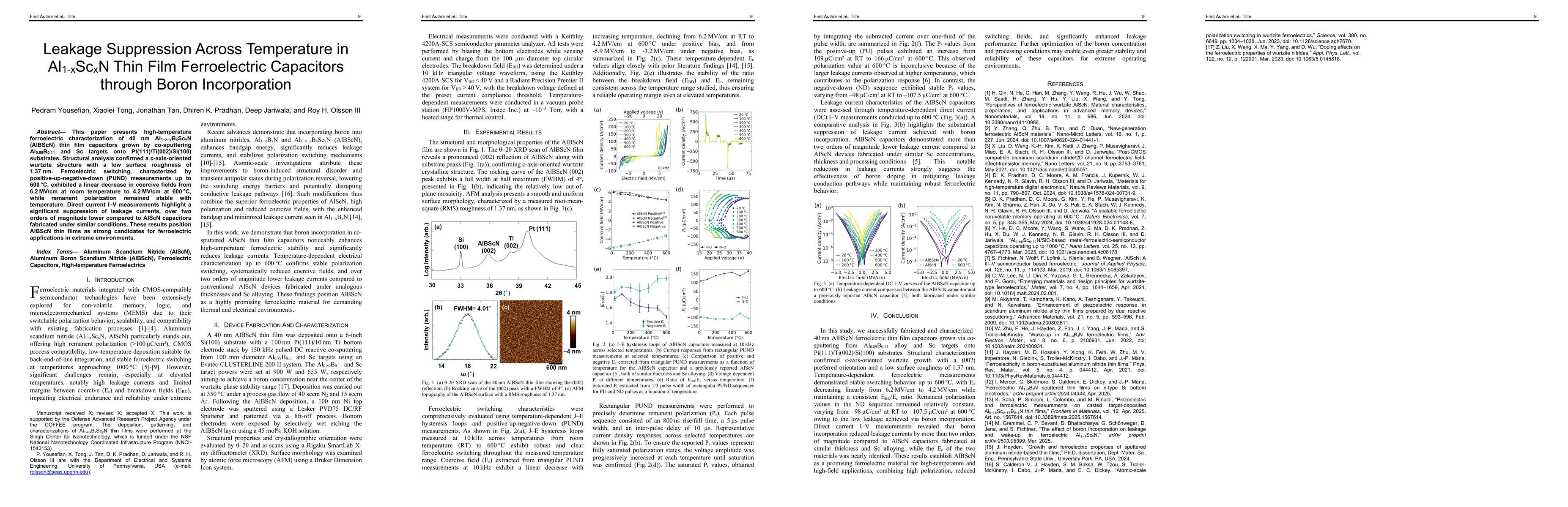
This paper presents high-temperature ferroelectric characterization of 40~nm Al$_{1-x-y}$B$_x$Sc$_y$N (AlBScN) thin film capacitors grown by co-sputtering Al$_{0.89}$B$_{0.11}$ and Sc targets onto Pt(...
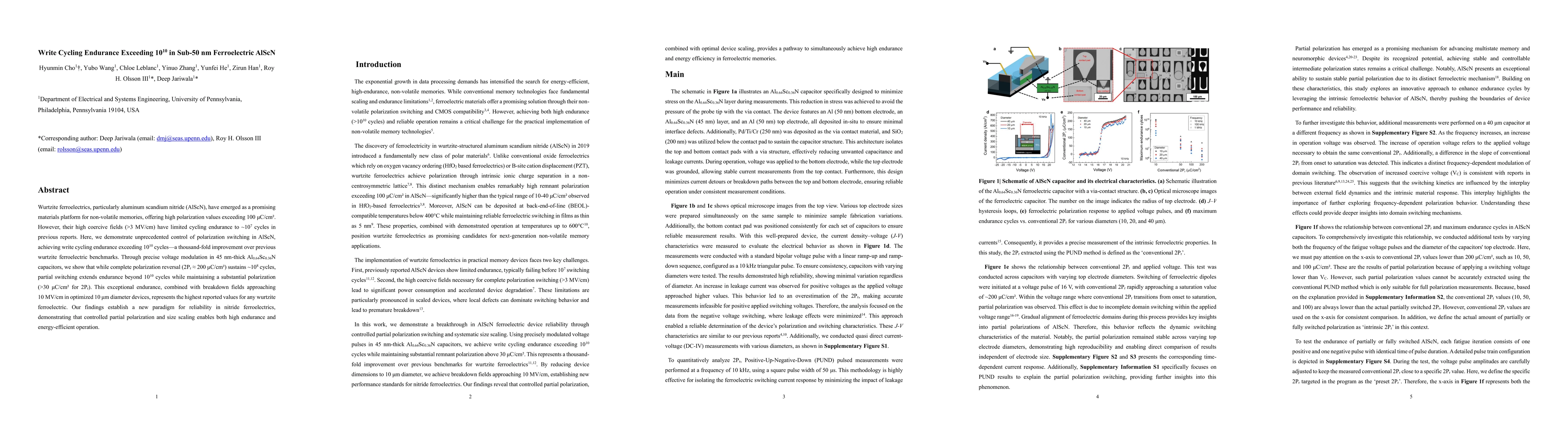
Wurtzite ferroelectrics, particularly aluminum scandium nitride (AlScN), have emerged as a promising materials platform for nonvolatile memories, offering high polarization values exceeding 100 uC/cm2...
Triggered by the development of exfoliation and the identification of a wide range of extraordinary physical properties in self-standing films consisting of one or few atomic layers, two-dimensional (...
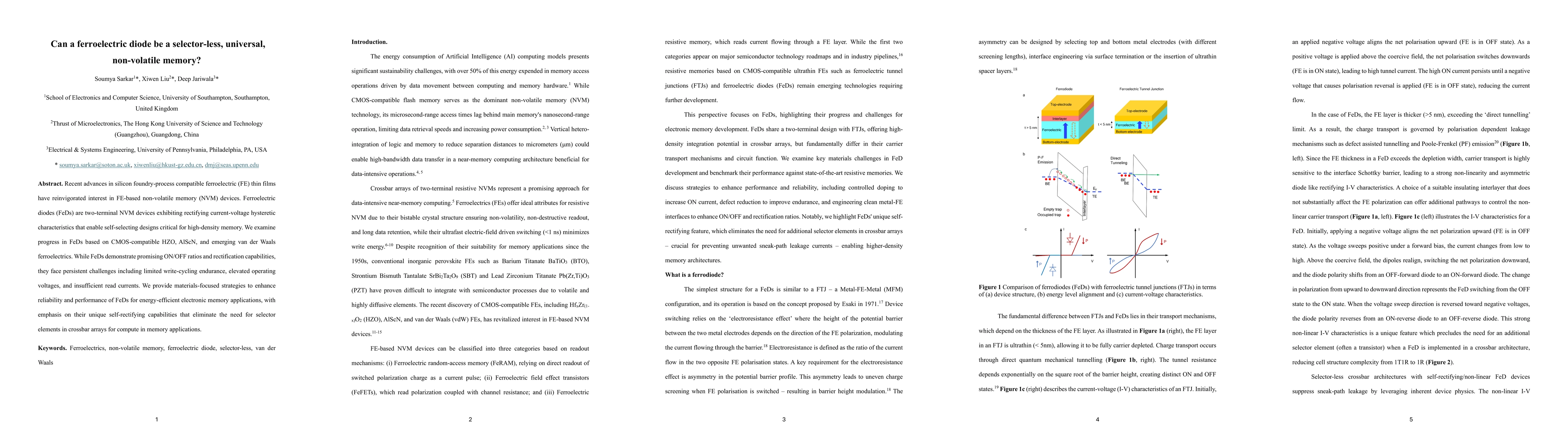
Recent advances in silicon foundry-process compatible ferroelectric (FE) thin films have reinvigorated interest in FE-based non-volatile memory (NVM) devices. Ferroelectric diodes (FeDs) are two-termi...
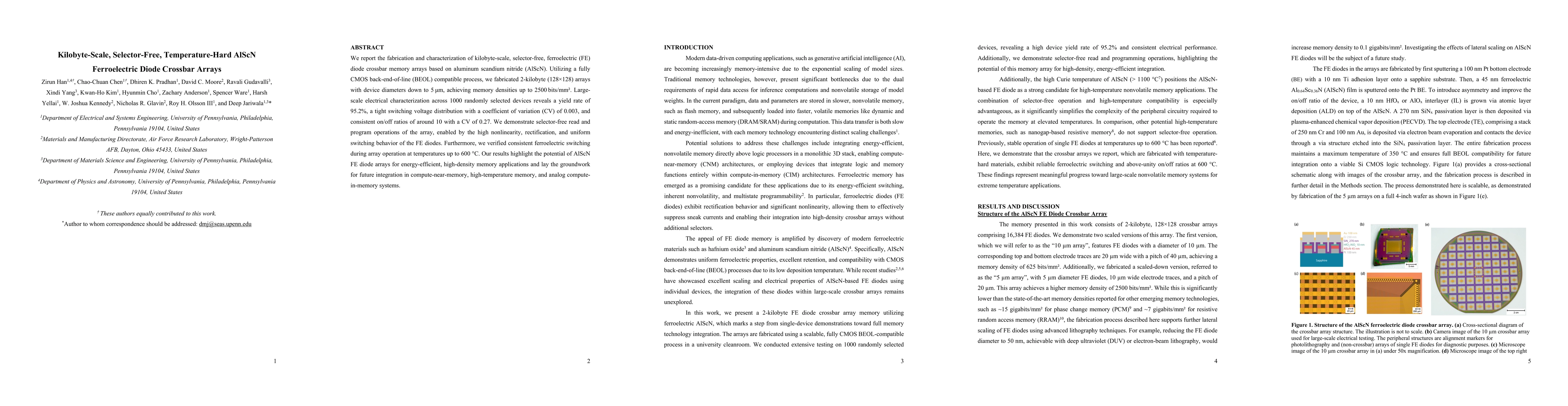
We report the fabrication and characterization of kilobyte-scale, selector-free, ferroelectric (FE) diode crossbar memory arrays based on aluminum scandium nitride (AlScN). Utilizing a fully CMOS back...
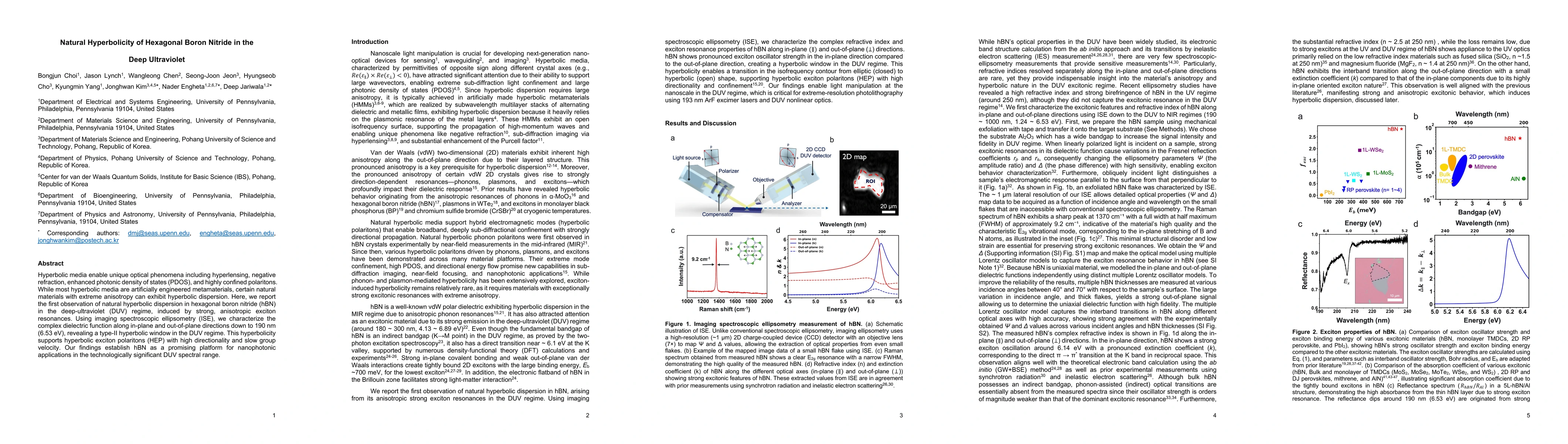
Hyperbolic media enable unique optical phenomena including hyperlensing, negative refraction, enhanced photonic density of states (PDOS), and highly confined polaritons. While most hyperbolic media ar...
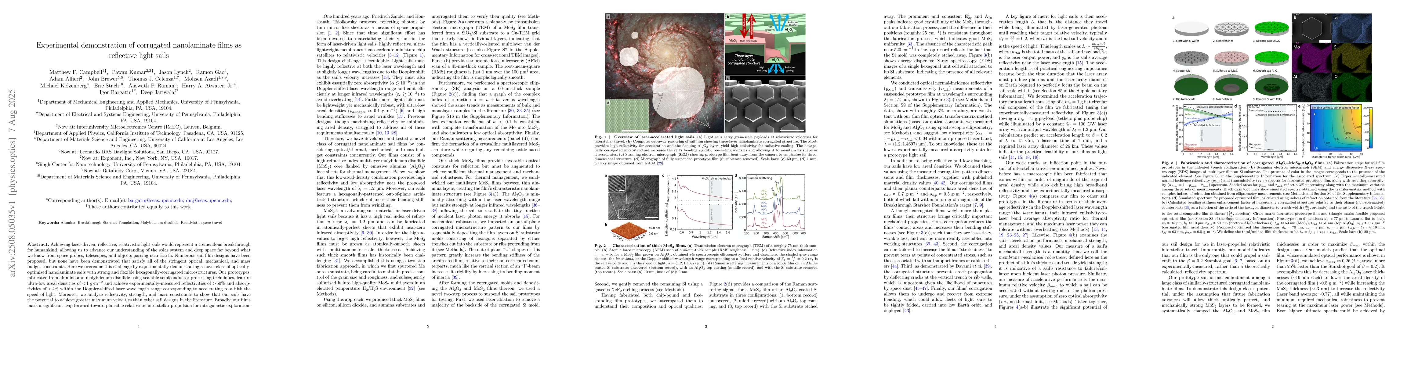
Achieving laser-driven, reflective, relativistic light sails would represent a tremendous breakthrough for humankind, allowing us to advance our understanding of the solar system and deep space far be...
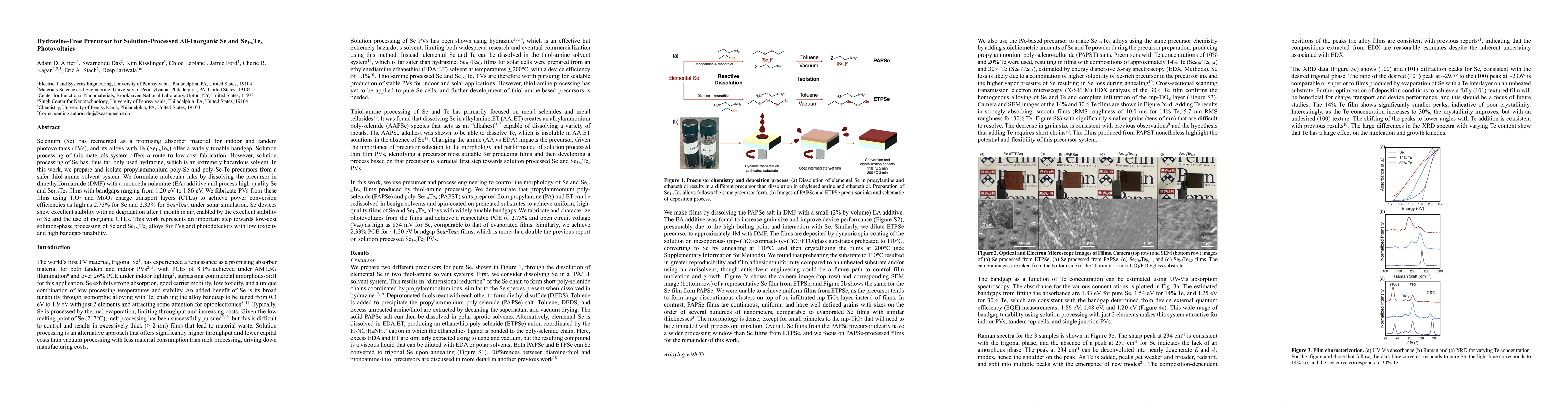
Selenium (Se) has reemerged as a promising absorber material for indoor and tandem photovoltaics (PVs), and its alloys with Te (Se1-xTex) offer a widely tunable bandgap. Solution processing of this ma...
Electrically tunable linear dichroism (LD) with non-volatile properties represents a critical yet elusive feature for next-generation integrated photonic elements in practical device architectures. He...
Metamaterials exhibiting hyperbolic dispersion enable unprecedented control over light-matter interactions, from sub-diffraction imaging to enhanced spontaneous emission. However, conventional plasmon...
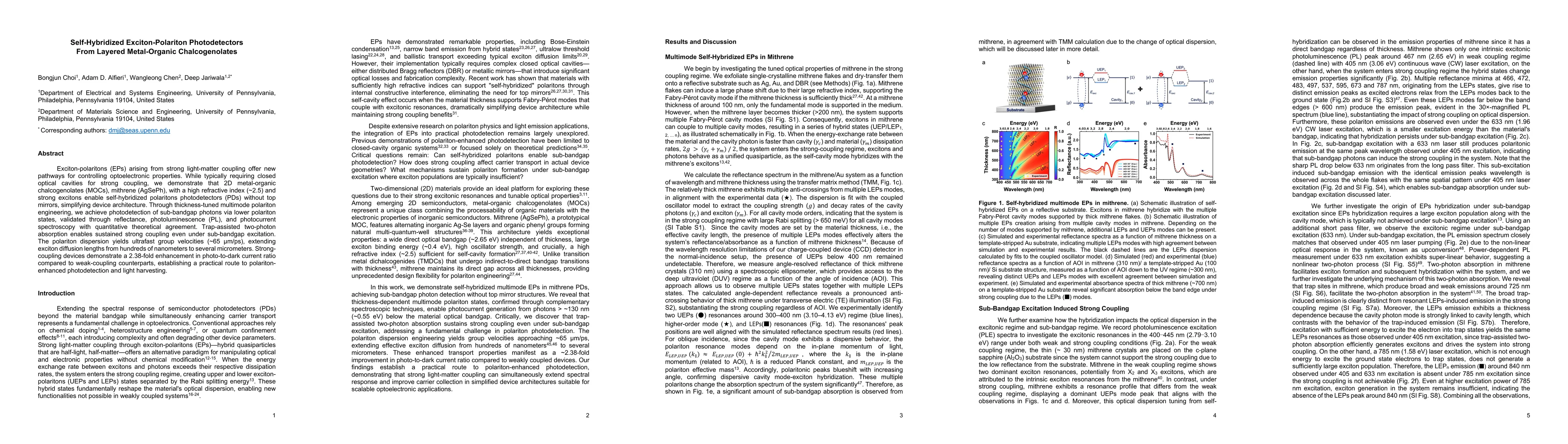
Exciton-polaritons (EPs) arising from strong light-matter coupling offer new pathways for controlling optoelectronic properties. While typically requiring closed optical cavities for strong coupling, ...
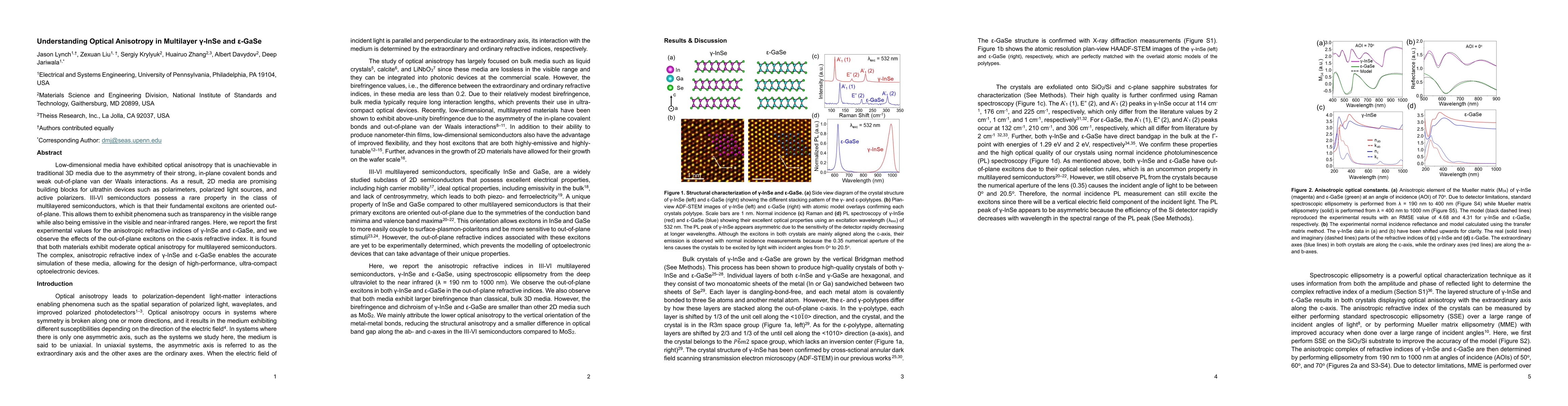
Low-dimensional media have exhibited optical anisotropy that is unachievable in traditional 3D media due to the asymmetry of their strong, in-plane covalent bonds and weak out-of-plane van der Waals i...
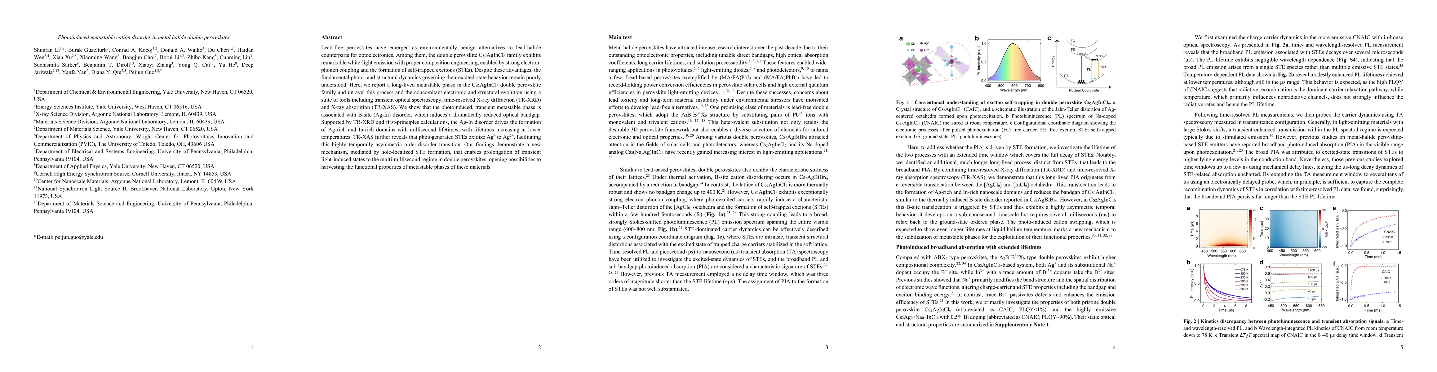
Lead-free perovskites have emerged as environmentally benign alternatives to lead-halide counterparts for optoelectronics. Among them, the double perovskite Cs2AgInCl6 family exhibits remarkable white...
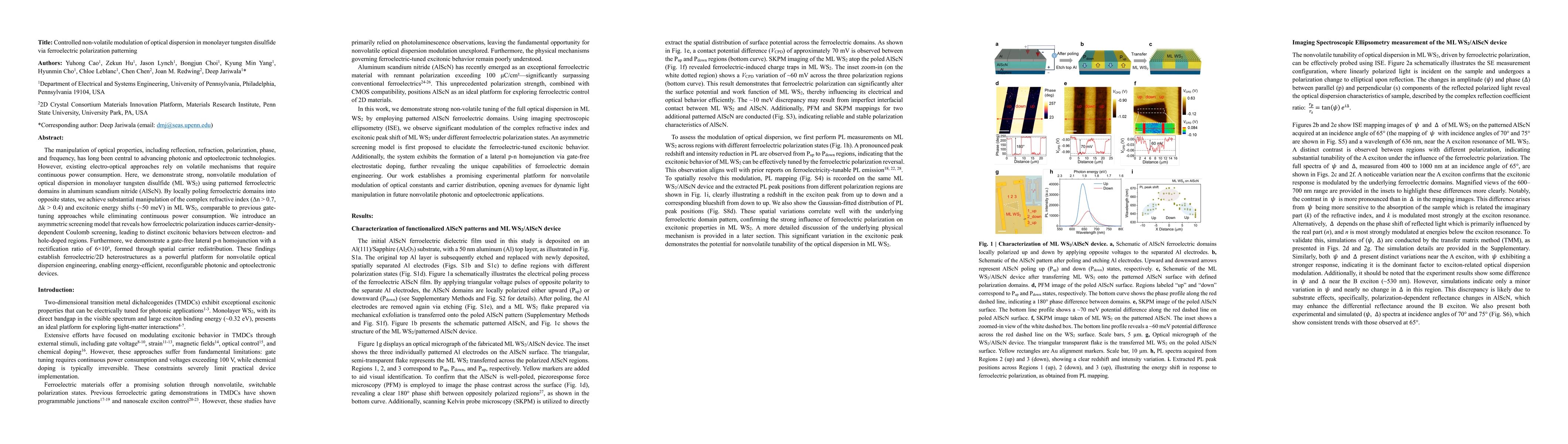
The manipulation of optical properties, including reflection, refraction, polarization, phase, and frequency, has long been central to advancing photonic and optoelectronic technologies. However, exis...
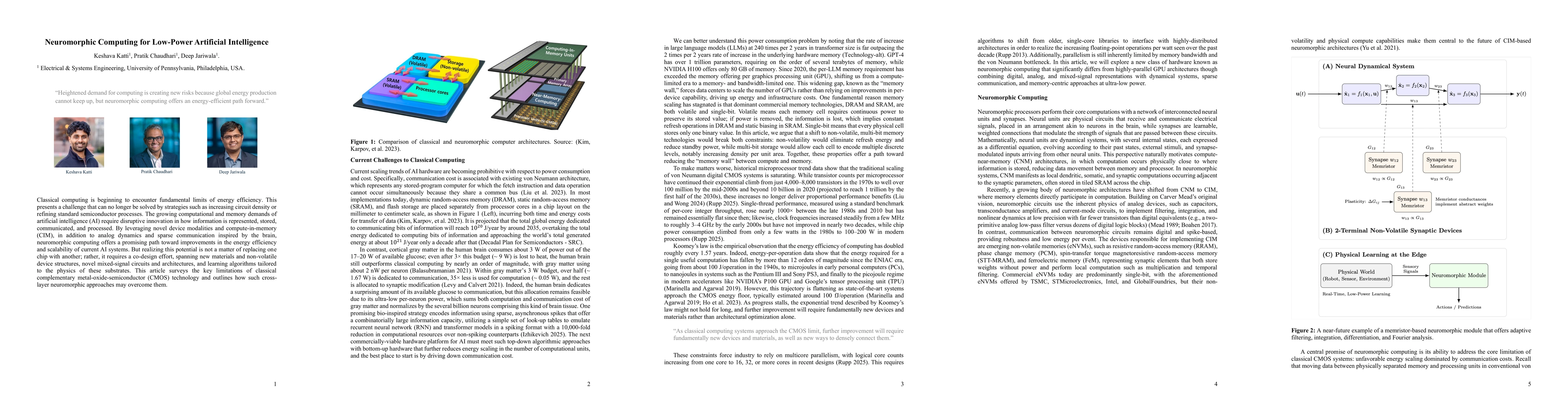
Classical computing is beginning to encounter fundamental limits of energy efficiency. This presents a challenge that can no longer be solved by strategies such as increasing circuit density or refini...
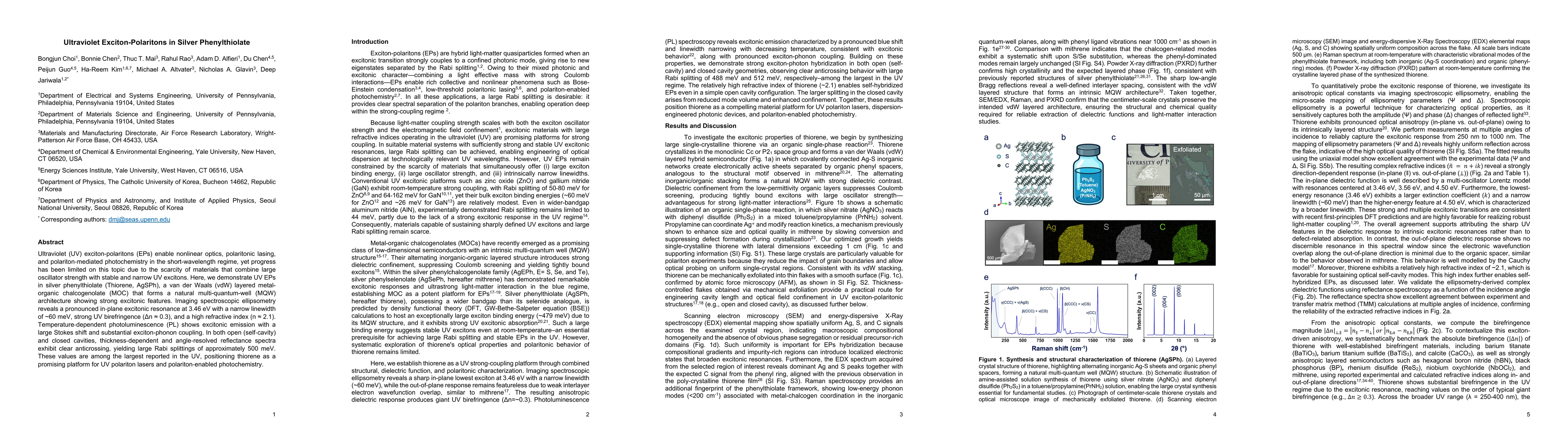
Ultraviolet (UV) exciton-polaritons (EPs) enable nonlinear optics, polaritonic lasing, and polariton-mediated photochemistry in the short-wavelength regime, yet progress has been limited due to the sc...
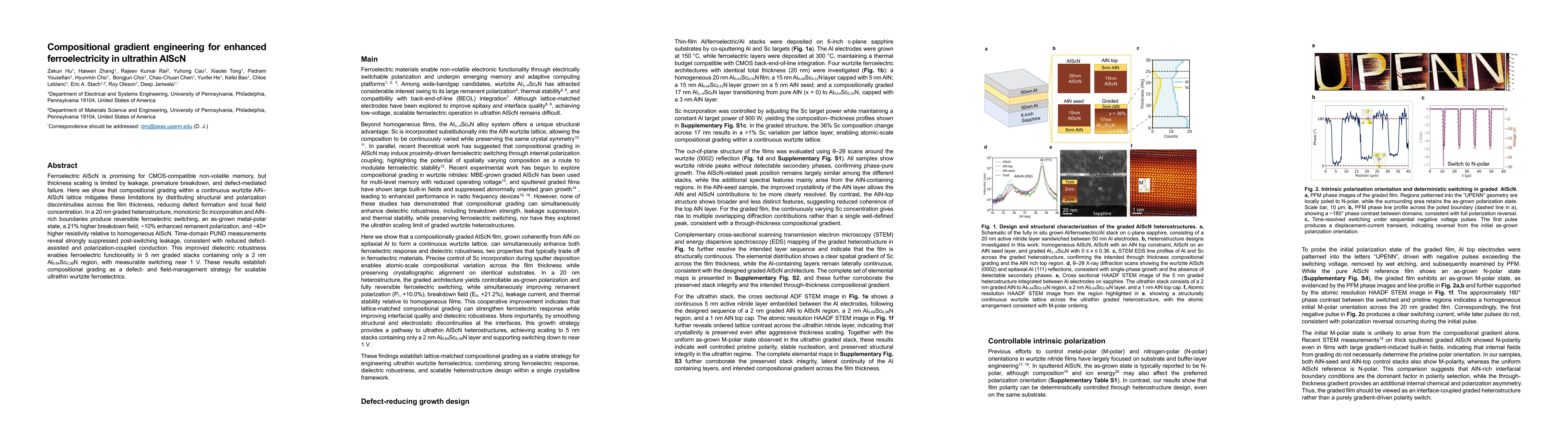
Ferroelectric AlScN is promising for CMOS-compatible non-volatile memory, but thickness scaling is limited by leakage, premature breakdown, and defect-mediated failure. Here we show that compositional...
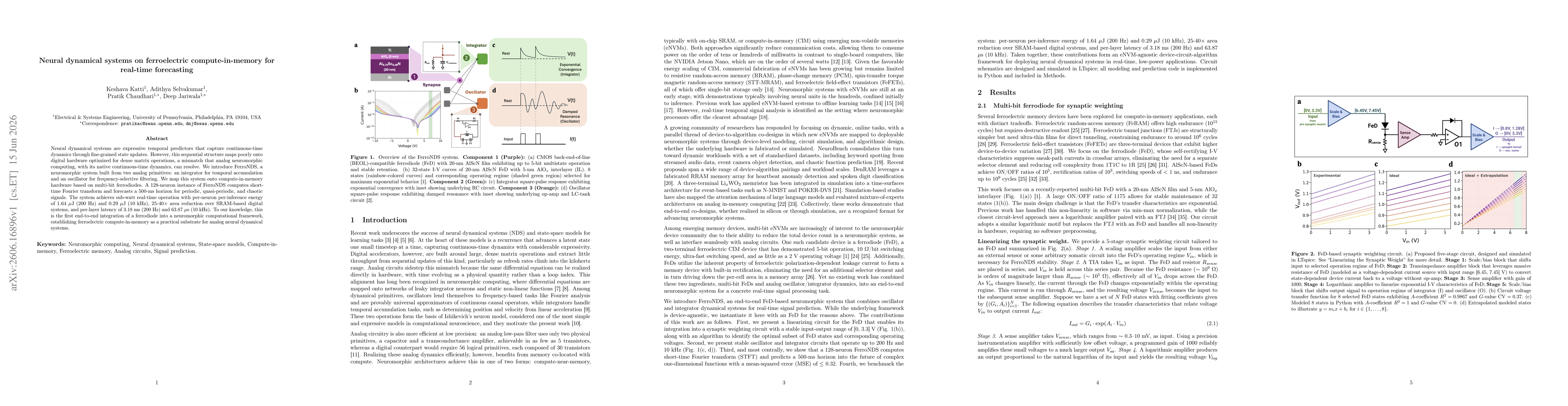
Neural dynamical systems are expressive temporal predictors that capture continuous-time dynamics through fine-grained state updates. However, this sequential structure maps poorly onto digital hardwa...