This paper demonstrates the successful scaling of Aluminum Scandium Nitride (AlScN) ferroelectric diode memory to 50 nm diameters, achieving a storage density of over 100 Mbit/mm$^2$. The study reveals a size-dependent behavior where switching voltage decreases while breakdown field increases, enhancing the breakdown-to-coercive field ratio, and enabling high-density memory applications.
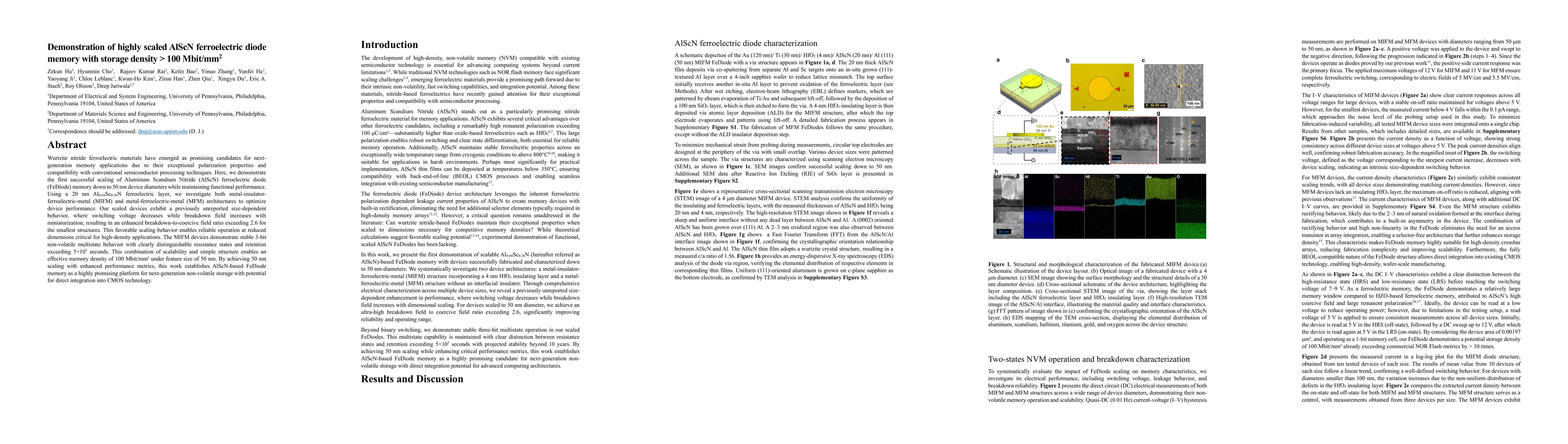
Wurtzite nitride ferroelectric materials have emerged as promising candidates for next-generation memory applications due to their exceptional polarization properties and compatibility with conventional semiconductor processing techniques. Here, we demonstrate the first successful scaling of Aluminum Scandium Nitride (AlScN) ferroelectric diode (FeDiode) memory down to 50 nm device diameters while maintaining functional performance. Using a 20 nm Al0.64Sc0.36N ferroelectric layer, we investigate both metal-insulator-ferroelectric-metal (MIFM) and metal-ferroelectric-metal (MFM) architectures to optimize device performance. Our scaled devices exhibit a previously unreported size-dependent behavior, where switching voltage decreases while breakdown field increases with miniaturization, resulting in an enhanced breakdown-to-coercive field ratio exceeding 2.6 for the smallest structures. This favorable scaling behavior enables reliable operation at reduced dimensions critical for high-density applications. The MIFM devices demonstrate stable 3-bit non-volatile multistate behavior with clearly distinguishable resistance states and retention exceeding $5\times 10^5$ seconds. This combination of scalability and simple structure enables an effective memory density of 100 Mbit/mm$^2$ under feature size of 50 nm. By achieving 50 nm scaling with enhanced performance metrics, this work establishes AlScN-based FeDiode memory as a highly promising platform for next-generation non-volatile storage with potential for direct integration into CMOS technology.
Generated Jun 09, 2025
The research methodology involved fabrication of MIFM and MFM devices using wet etching, spin coating, electron beam lithography, dry etching, and deposition of dielectric and electrode materials via PECVD, ALD, and thermal evaporation, followed by lift-off processes.
This work establishes AlScN-based FeDiode memory as a highly promising platform for next-generation non-volatile storage with potential for direct integration into CMOS technology, due to its high storage density (>100 Mbit/mm²) and favorable scaling behavior.
The paper presents the first successful scaling of AlScN ferroelectric diode memory to 50 nm device diameters, demonstrating size-dependent behavior and stable multistate operation.
The research introduces a novel approach to scaling ferroelectric memory devices using AlScN, showcasing enhanced breakdown-to-coercive field ratio and high storage density, which is critical for high-density non-volatile memory applications.
No key terms available for this paper.
Current paper (gray), citations (green), references (blue)
Hermann Kohlstedt, Niklas Wolff, Georg Schönweger et al.
L. Li, H. Lee, J. Encomendero et al.
Deep Jariwala, Xiwen Liu, Soumya Sarkar
No citations found for this paper.
Comments (0)