Kyeongjae Cho

9 papers on arXiv

Academic Profile

Name: K. Cho
Total Papers: 2

Statistics

arXiv Papers 9
Total Publications 2

Papers on arXiv

Thumbnail for Direct imaging of asymmetric interfaces and electrostatic potentials
  inside a hafnia-zirconia ferroelectric nanocapacitor

Direct imaging of asymmetric interfaces and electrostatic potentials inside a hafnia-zirconia ferroelectric nanocapacitor

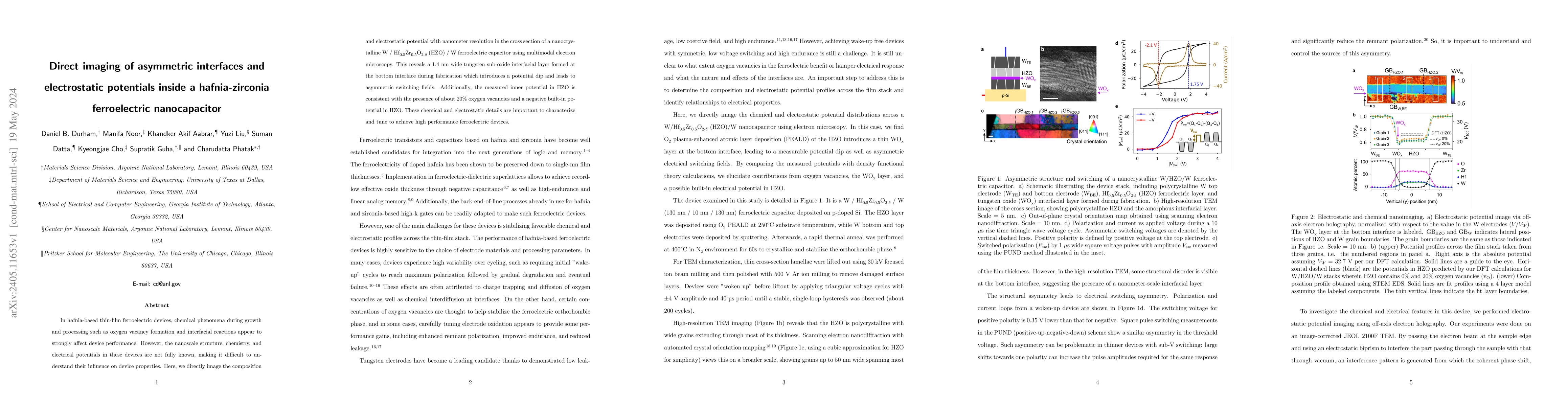
In hafnia-based thin-film ferroelectric devices, chemical phenomena during growth and processing such as oxygen vacancy formation and interfacial reactions appear to strongly affect device performan...

Thumbnail for Seamless monolithic three-dimensional integration of single-crystalline
  films by growth

Seamless monolithic three-dimensional integration of single-crystalline films by growth

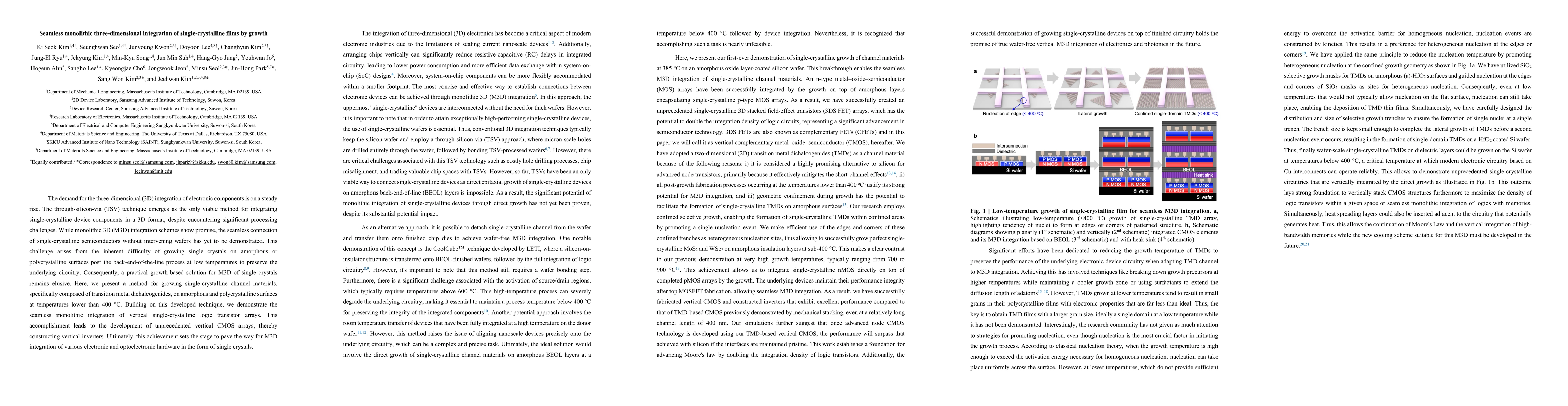
The demand for the three-dimensional (3D) integration of electronic components is on a steady rise. The through-silicon-via (TSV) technique emerges as the only viable method for integrating single-c...

Thumbnail for Two Types of 3D Quantum Hall Effects in Multilayer WTe$_2$

Two Types of 3D Quantum Hall Effects in Multilayer WTe$_2$

Interplay between the topological surface states and bulk states gives rise to diverse exotic transport phenomena in topological materials. The recently proposed Weyl orbit in topological semimetals...

Thumbnail for A Nanometer-Thick Oxide Semiconductor Transistor with Ultra-High Drain
  Current

A Nanometer-Thick Oxide Semiconductor Transistor with Ultra-High Drain Current

High drive current is a critical performance parameter in semiconductor devices for high-speed, low-power logic applications or high-efficiency, high-power, high-speed radio frequency (RF) analog ap...

Thumbnail for Why In2O3 Can Make 0.7 nm Atomic Layer Thin Transistors?

Why In2O3 Can Make 0.7 nm Atomic Layer Thin Transistors?

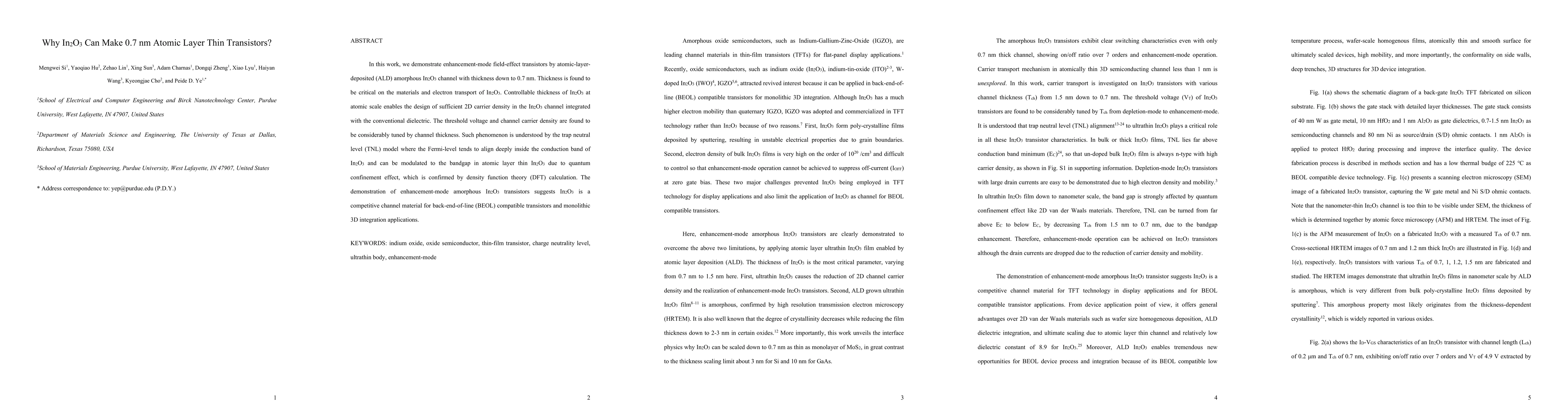
In this work, we demonstrate enhancement-mode field-effect transistors by atomic-layer-deposited (ALD) amorphous In2O3 channel with thickness down to 0.7 nm. Thickness is found to be critical on the...

Thumbnail for Flatbands and Mechanical Deformation Effects in the Moir\'e Superlattice
  of MoS$_2$-WSe$_2$ Heterobilayers

Flatbands and Mechanical Deformation Effects in the Moir\'e Superlattice of MoS$_2$-WSe$_2$ Heterobilayers

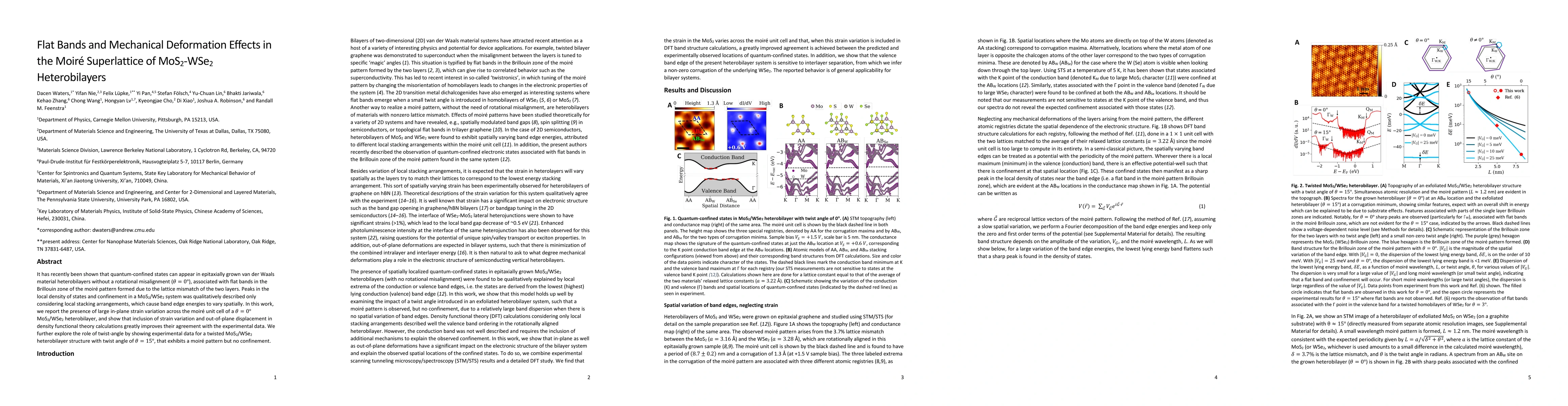
It has recently been shown that quantum-confined states can appear in epitaxially grown van der Waals material heterobilayers without a rotational misalignment ($\theta=0^\circ$), associated with fl...

Thumbnail for Real-time ab initio simulation of inelastic electron scattering using
  the exact, density functional, and alternative approaches

Real-time ab initio simulation of inelastic electron scattering using the exact, density functional, and alternative approaches

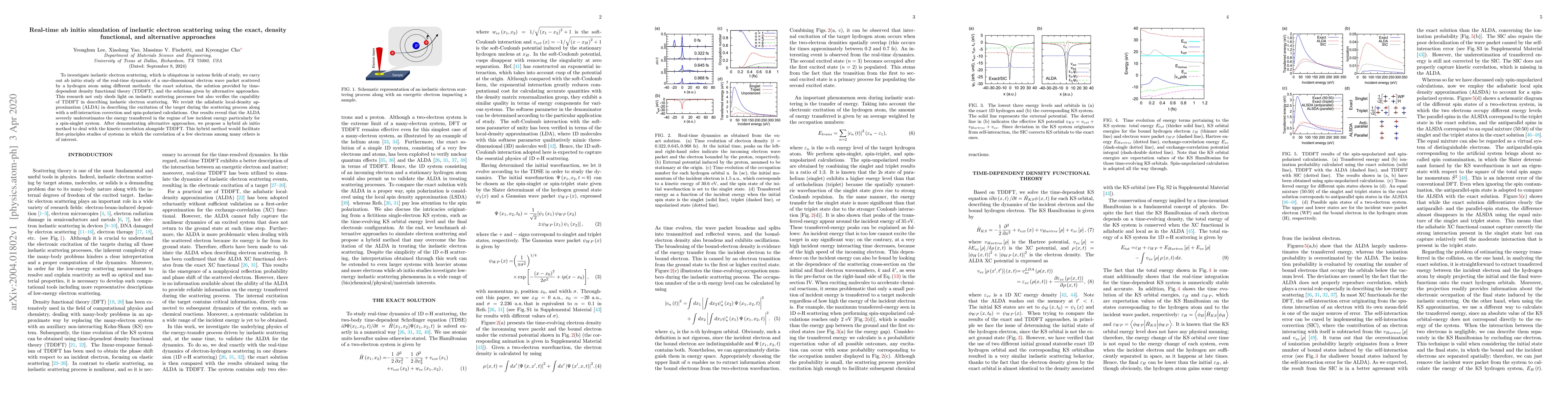
To investigate inelastic electron scattering, which is ubiquitous in various fields of study, we carry out ab initio study of the real-time dynamics of a one-dimensional electron wave packet scatter...

Thumbnail for Atomic-scale confinement of strongly charged 180 degree domain wall
  pairs in ZrO2

Atomic-scale confinement of strongly charged 180 degree domain wall pairs in ZrO2

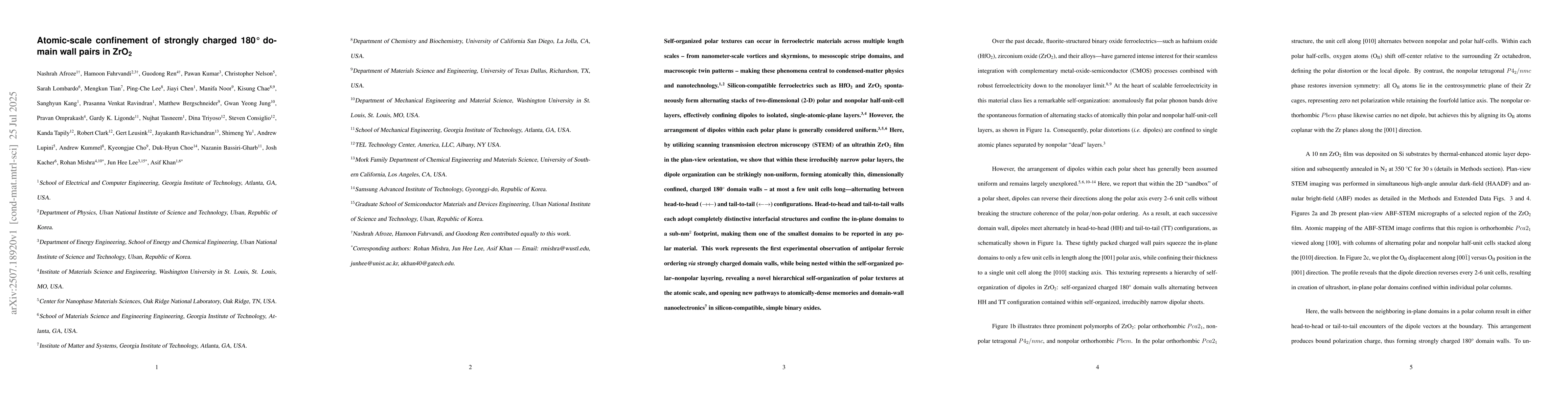
Self organized polar textures can occur in ferroelectric materials across multiple length scales, from nanometer scale vortices and skyrmions, to mesoscopic stripe domains, and macroscopic twin patter...

Thumbnail for Role of surface states and band modulations in ultrathin ruthenium interconnects

Role of surface states and band modulations in ultrathin ruthenium interconnects

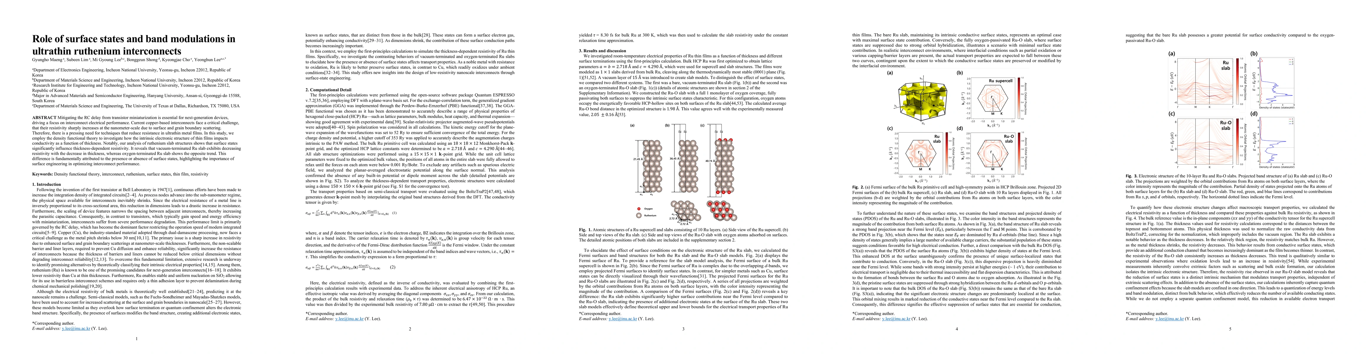
Mitigating the RC delay from transistor miniaturization is essential for next-generation devices, driving a focus on interconnect electrical performance. Current copper-based interconnects face a crit...

This website uses cookies to ensure you get the best experience. Learn more