Academic Profile
Statistics
Similar Authors
Papers on arXiv
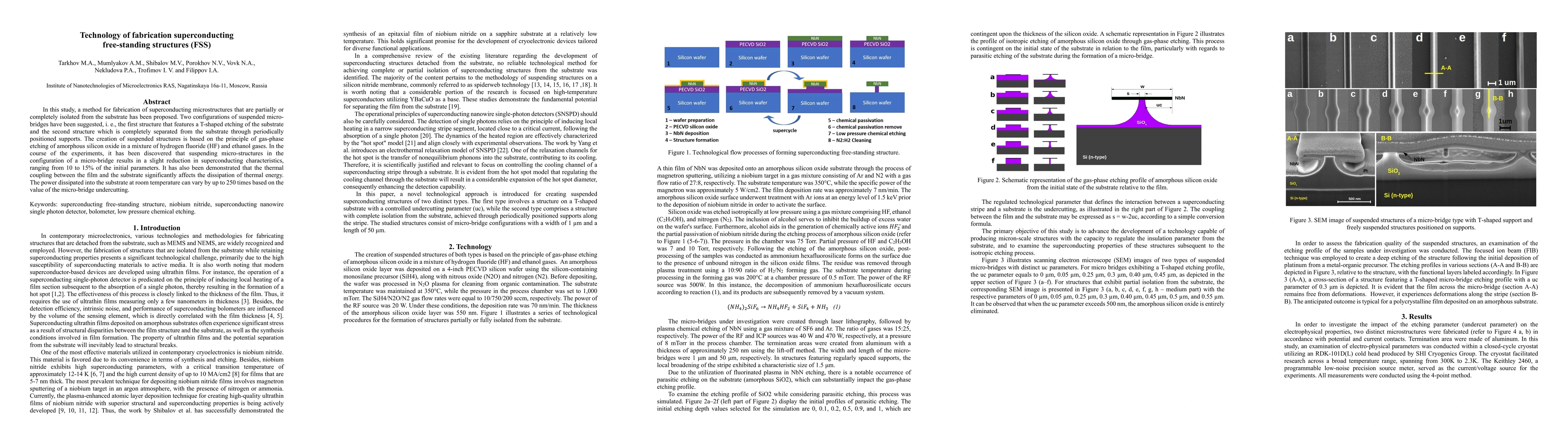
In this study, a method for fabrication of superconducting microstructures that are partially or completely isolated from the substrate has been proposed. Two configurations of suspended microbridge...
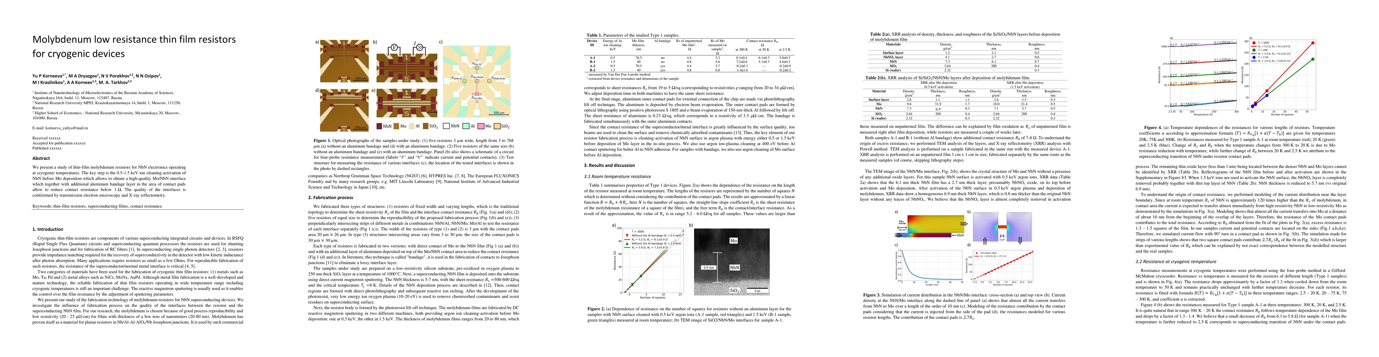
We present a study of thin-film molybdenum resistors for NbN electronics operating at cryogenic temperatures. The key step is the 0.5-1.5 keV ion cleaning-activation of NbN before Mo deposition whic...
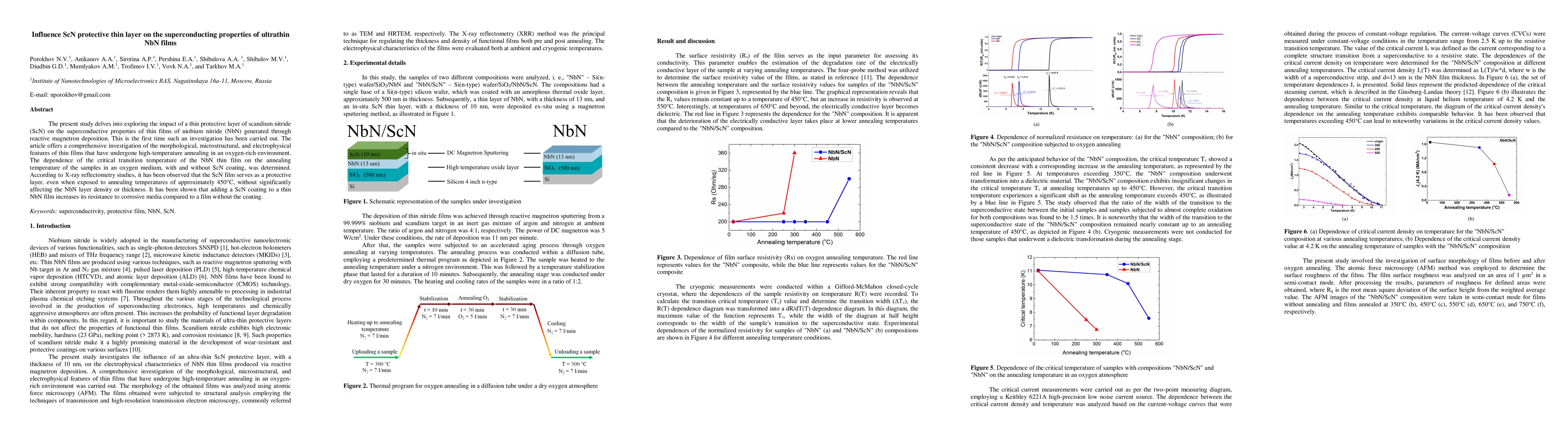
The present study delves into exploring the impact of a thin protective layer of scandium nitride (ScN) on the superconductive properties of thin films of niobium nitride (NbN) generated through rea...
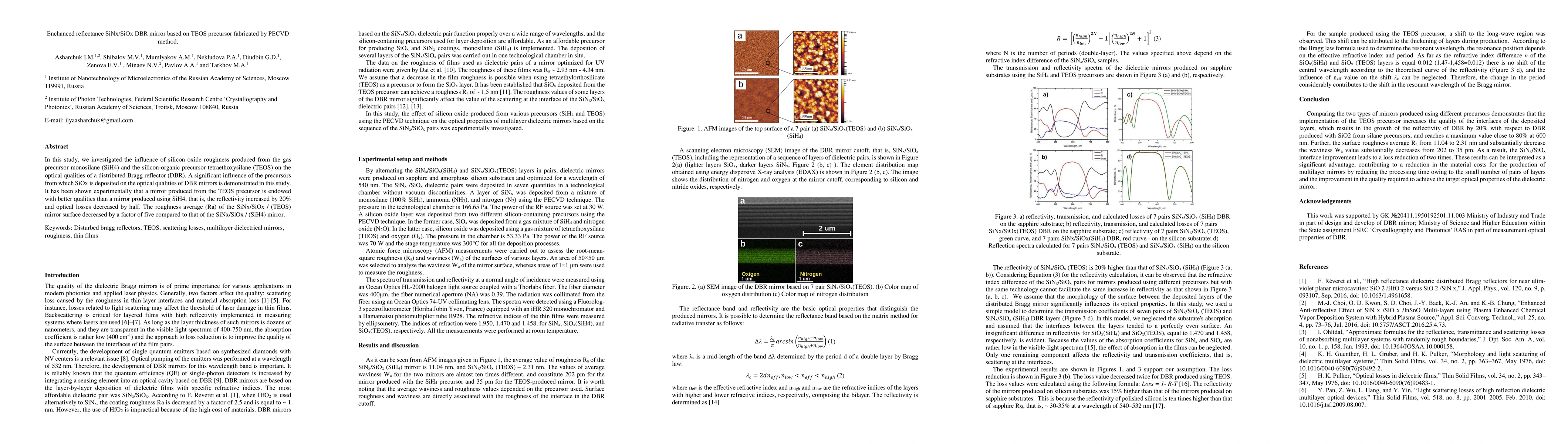
In this study, we investigated the influence of silicon oxide roughness produced from the gas precursor monosilane (SiH$_4$) and the silicon-organic precursor tetraethoxysilane (TEOS) on the optical...
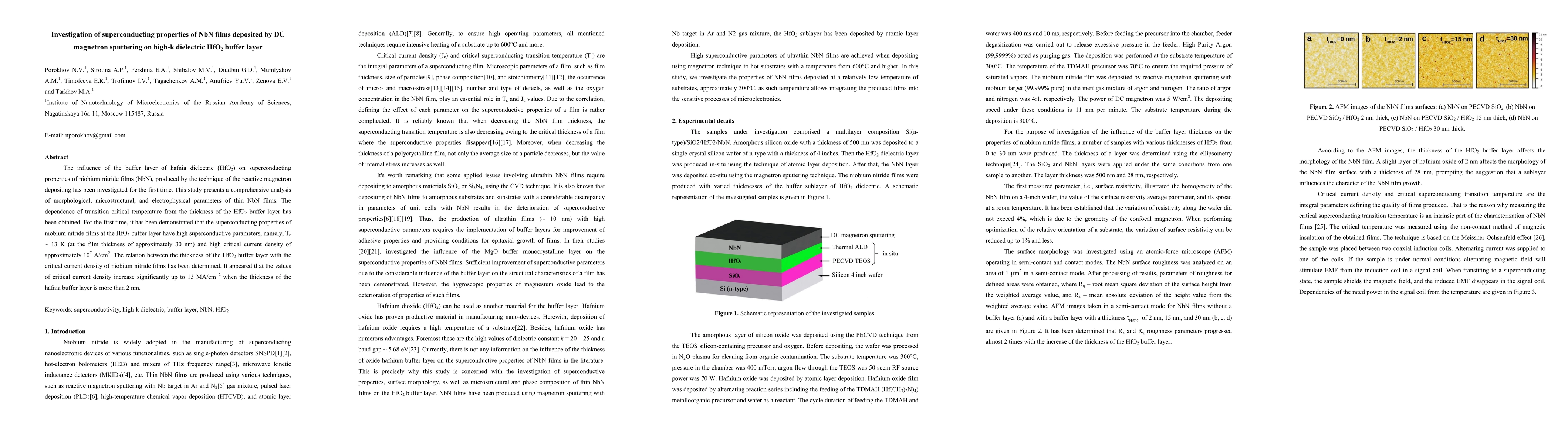
The influence of the buffer layer of hafnia dielectric on superconducting properties of niobium nitride films, produced by the technique of the reactive magnetron depositing has been investigated fo...
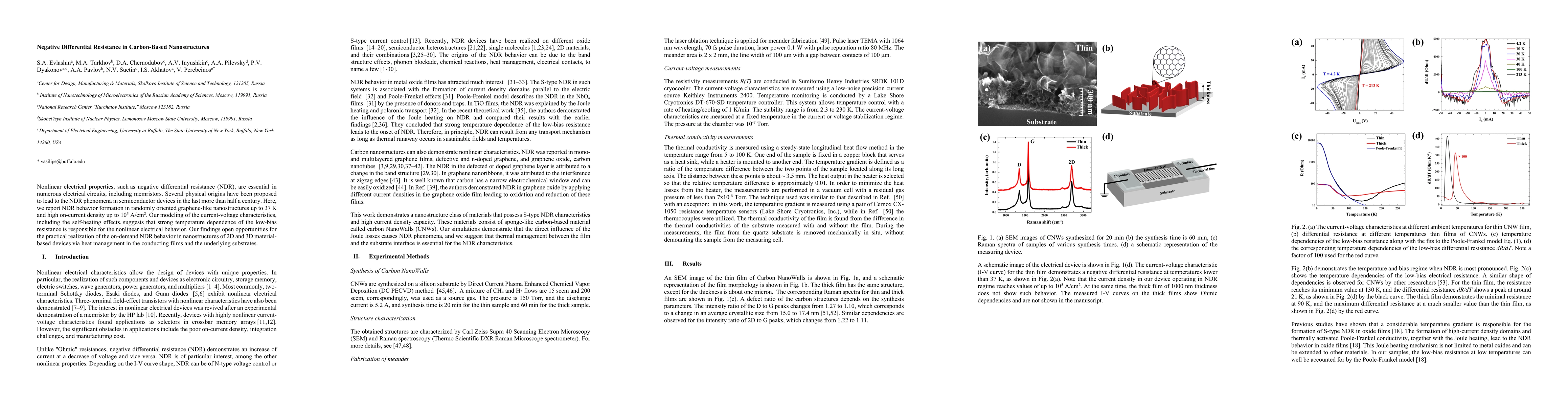
Nonlinear electrical properties, such as negative differential resistance (NDR), are essential in numerous electrical circuits, including memristors. Several physical origins have been proposed to l...
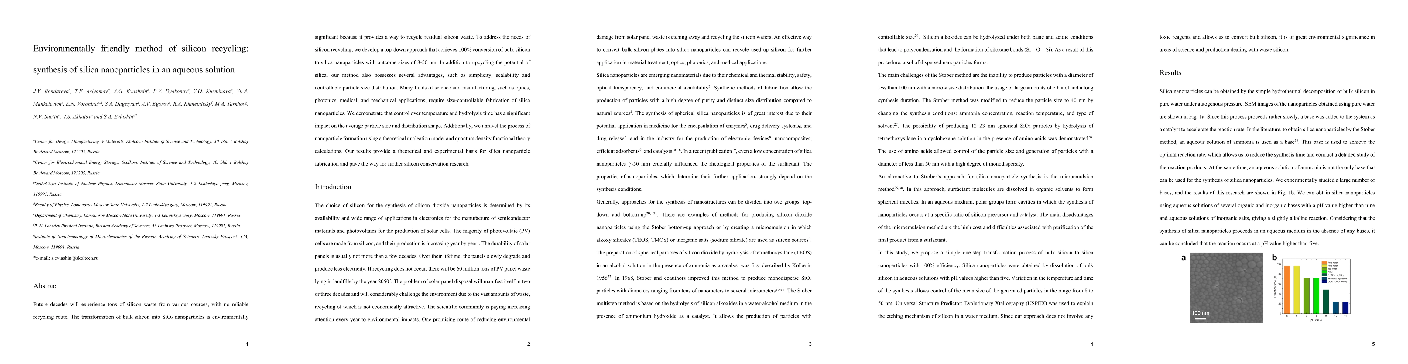
Future decades will experience tons of silicon waste from various sources, with no reliable recycling route. The transformation of bulk silicon into SiO2 nanoparticles is environmentally significant...
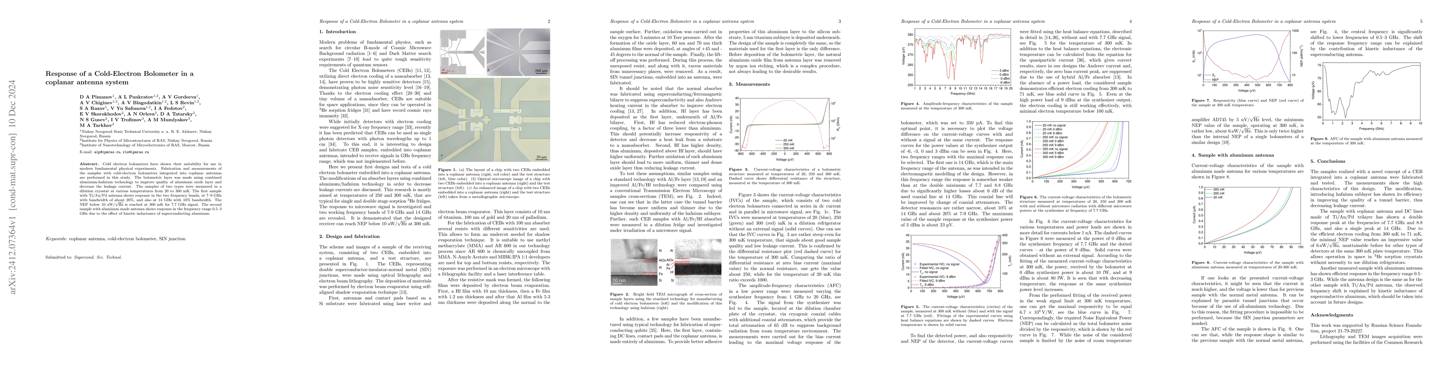
Cold electron bolometers have shown their suitability for use in modern fundamental physical experiments. Fabrication and measurements of the samples with cold-electron bolometers integrated into copl...
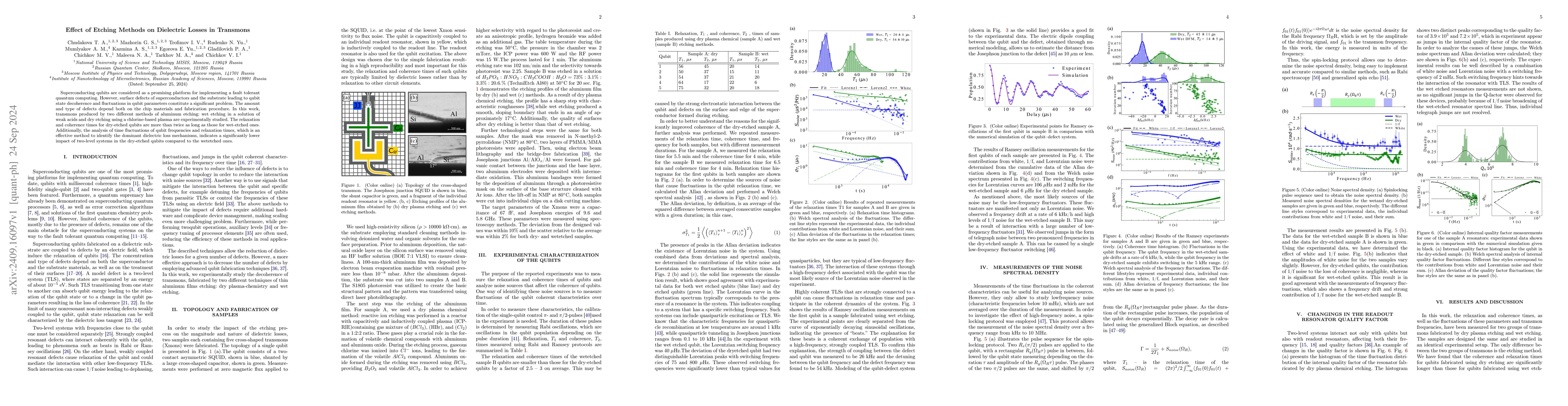
Superconducting qubits are considered as a promising platform for implementing a fault tolerant quantum computing. However, surface defects of superconductors and the substrate leading to qubit state ...
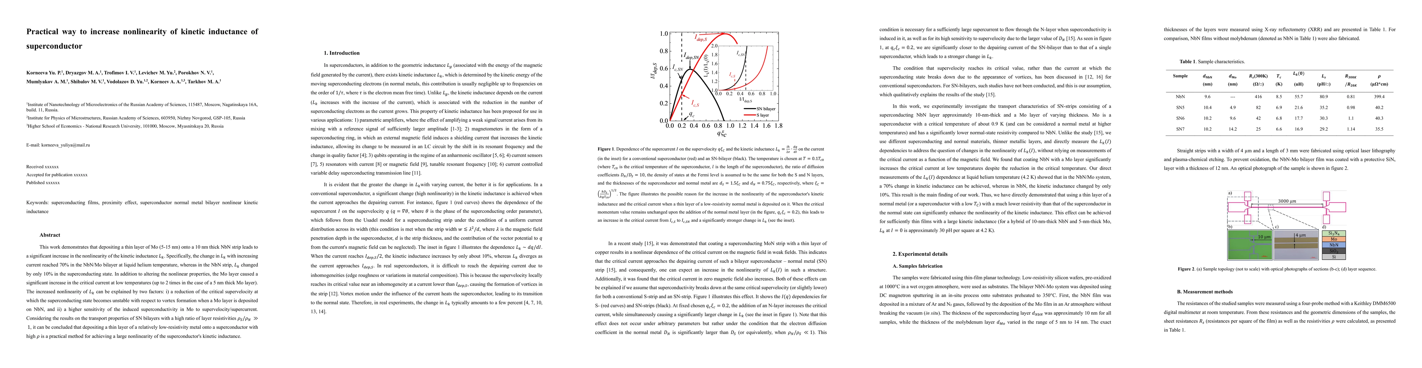
This work demonstrates that depositing a thin layer of Mo (5-15 nm) onto a 10 nm thick NbN strip leads to a significant increase in the nonlinearity of the kinetic inductance $L_k$. Specifically, the ...
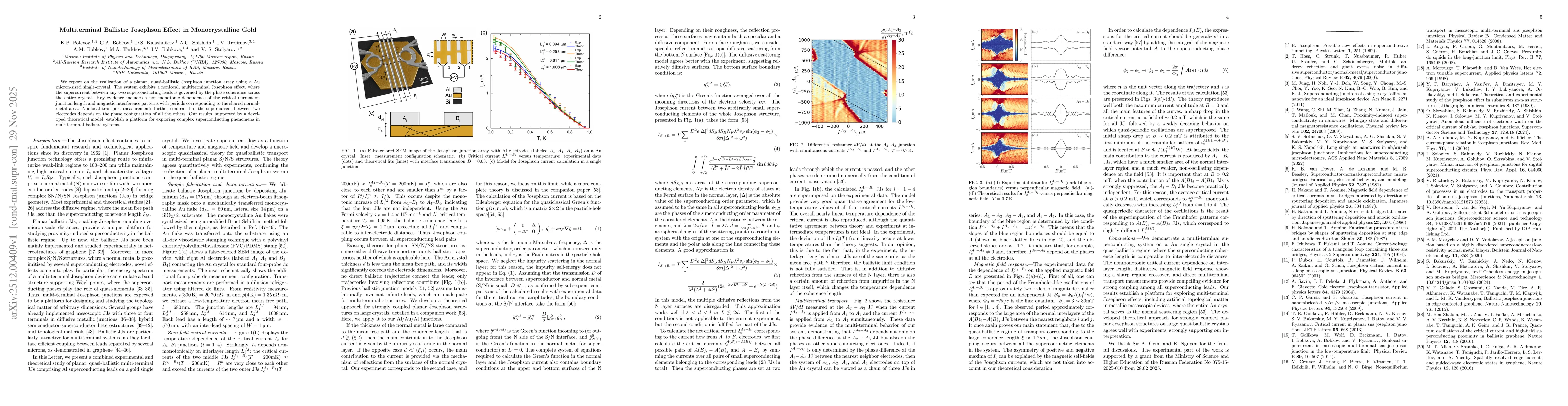
We report on the realization of a planar, quasi-ballistic Josephson junction array using a Au micron-sized single-crystal. The system exhibits a nonlocal, multiterminal Josephson effect, where the sup...
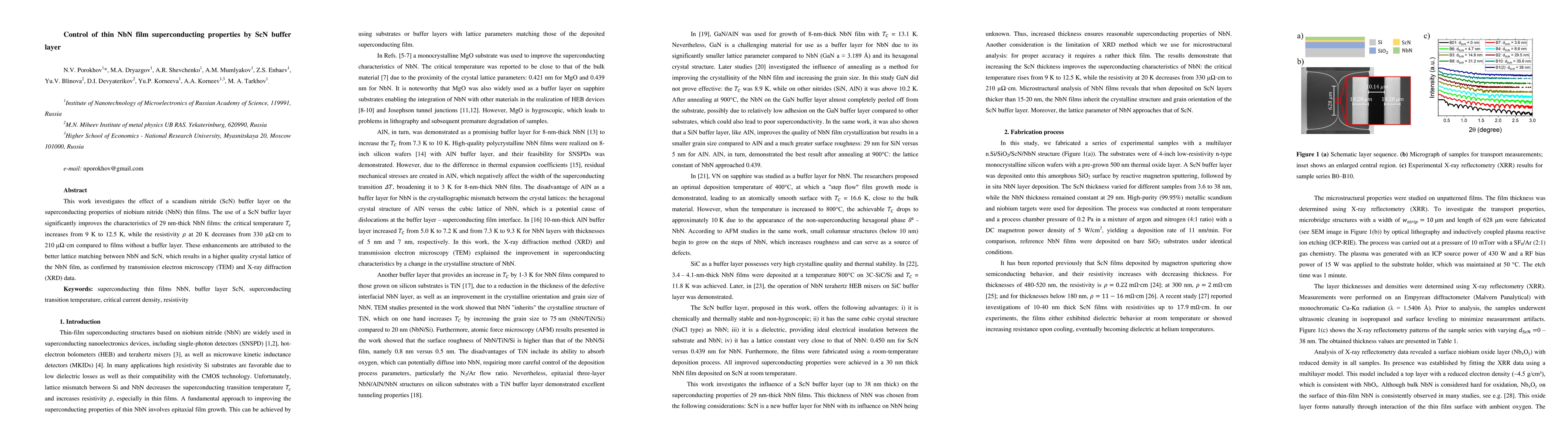
This work investigates the effect of a scandium nitride buffer layer on the superconducting properties of niobium nitride thin films. The use of a ScN buffer layer significantly improves the character...
In this work, we design and characterize a 4-pixel superconducting hot-electron bolometer (HEB) based on niobium nitride (NbN), integrated with individual planar silicon nitride (Si$_3$N$_4$) waveguid...