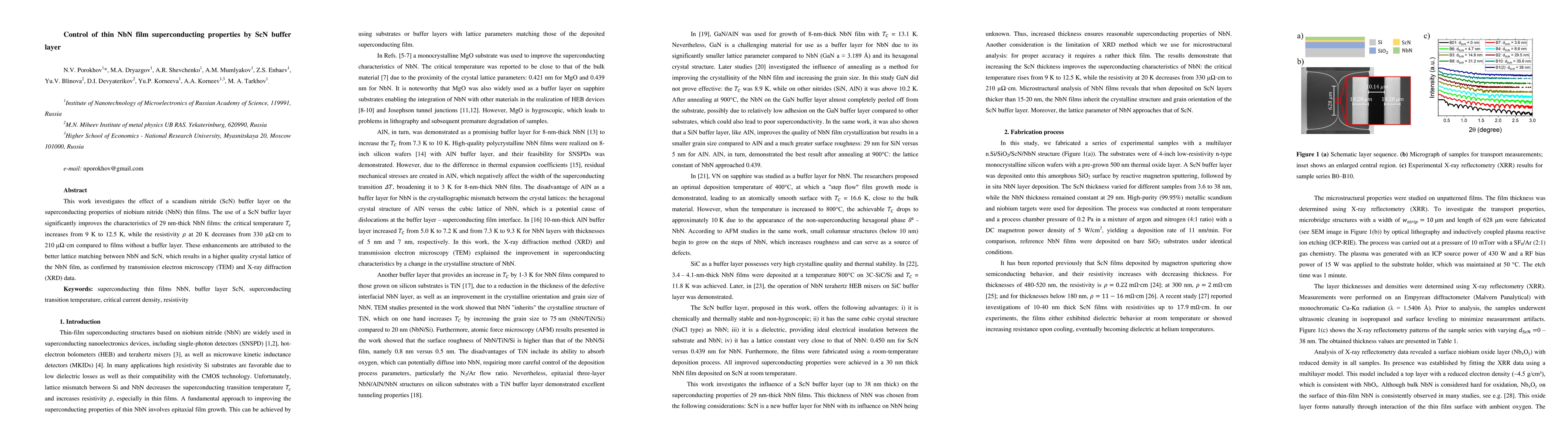
ArxivLens

Publication

Published: Dec 15, 2025
Categories: cond-mat.supr-con

Metrics

Source: ArXiv

Quick Answers

What methodology did the authors use?

The study employed magnetron sputtering to deposit NbN films with ScN buffer layers. Transport measurements, including resistance and critical current analysis, were conducted using a cryocooler and Keithley SourceMeter. TEM and XRD analyses were used to examine microstructure and lattice parameters. More in Methodology →

What are the key results?

Critical temperature (Tc) increased from 9 K to 12.5 K with ScN buffer layer — Resistivity at 20 K decreased from 330 μΩ·cm to 210 μΩ·cm More in Key Results →

Why is this work significant?

This research demonstrates significant enhancement of NbN superconducting properties through ScN buffer layer, which could improve performance of superconducting devices like SNSPDs for quantum technologies More in Significance →

What are the main limitations?

Limited data on long-term stability of NbN/ScN interfaces — No detailed analysis of thermal expansion mismatch between layers More in Limitations →

Paper Preview

Abstract

This work investigates the effect of a scandium nitride buffer layer on the superconducting properties of niobium nitride thin films. The use of a ScN buffer layer significantly improves the characteristics of 29 nm thick NbN films: the critical temperature Tc increases from 9 K to 12.5 K, while the resistivity at 20 K decreases from 330 mkOhm*cm to 210 mkOhm*cm compared to films without a buffer layer. These enhancements are attributed to the better lattice matching between NbN and ScN, which results in a higher quality crystal lattice of the NbN film, as confirmed by transmission electron microscopy and X-ray diffraction data.

Key Findings, in focus

Seven facets of this paper, analysed and brought into focus by AI.

AI-generated · verify against source Generated Dec 17, 2025
In focus · one-line synthesis

This research demonstrates significant enhancement of NbN superconducting properties through ScN buffer layer, which could improve performance of superconducting devices like SNSPDs for quantum technologies

01
MethodologyHow they did it

The study employed magnetron sputtering to deposit NbN films with ScN buffer layers. Transport measurements, including resistance and critical current analysis, were conducted using a cryocooler and Keithley SourceMeter. TEM and XRD analyses were used to examine microstructure and lattice parameters.

02
ResultsWhat they found
  • Critical temperature (Tc) increased from 9 K to 12.5 K with ScN buffer layer
  • Resistivity at 20 K decreased from 330 μΩ·cm to 210 μΩ·cm
  • Maximum critical current density reached ~8 MA/cm²
03
SignificanceWhy it matters

This research demonstrates significant enhancement of NbN superconducting properties through ScN buffer layer, which could improve performance of superconducting devices like SNSPDs for quantum technologies

04
Technical ContributionsWhat's new technically

Development of a method to enhance NbN superconducting properties through controlled ScN buffer layer integration

05
NoveltyWhat sets it apart

First demonstration of ScN buffer layer significantly improving NbN film superconducting properties through lattice matching and columnar structure formation

06
LimitationsWhat to be cautious about
  • Limited data on long-term stability of NbN/ScN interfaces
  • No detailed analysis of thermal expansion mismatch between layers
07
Future WorkWhere it goes next
  • Investigate long-term stability and degradation mechanisms of NbN/ScN interfaces
  • Explore optimization of ScN thickness for specific device applications

Paper Details

Paper ID: 2512.13367
Categories:
cond-mat.supr-con

How to Cite This Paper

Reference manager: RIS EndNote


Discussion 0

This website uses cookies to ensure you get the best experience. Learn more