Academic Profile
Statistics
Similar Authors
Papers on arXiv
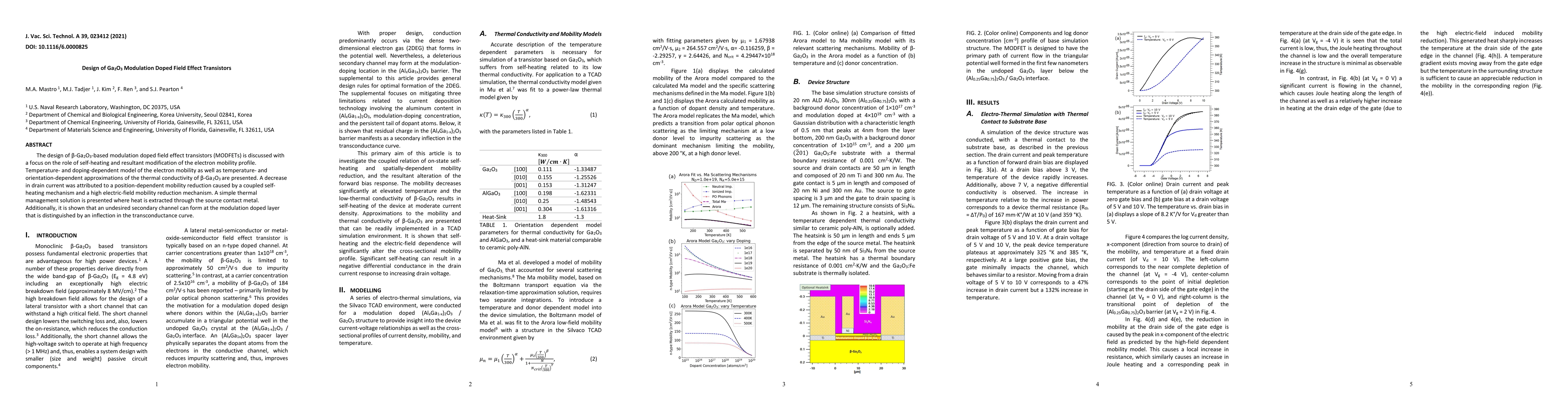
The design of beta-Ga2O3-based modulation doped field effect transistors (MODFETs) is discussed with a focus on the role of self-heating and resultant modification of the electron mobility profile. ...
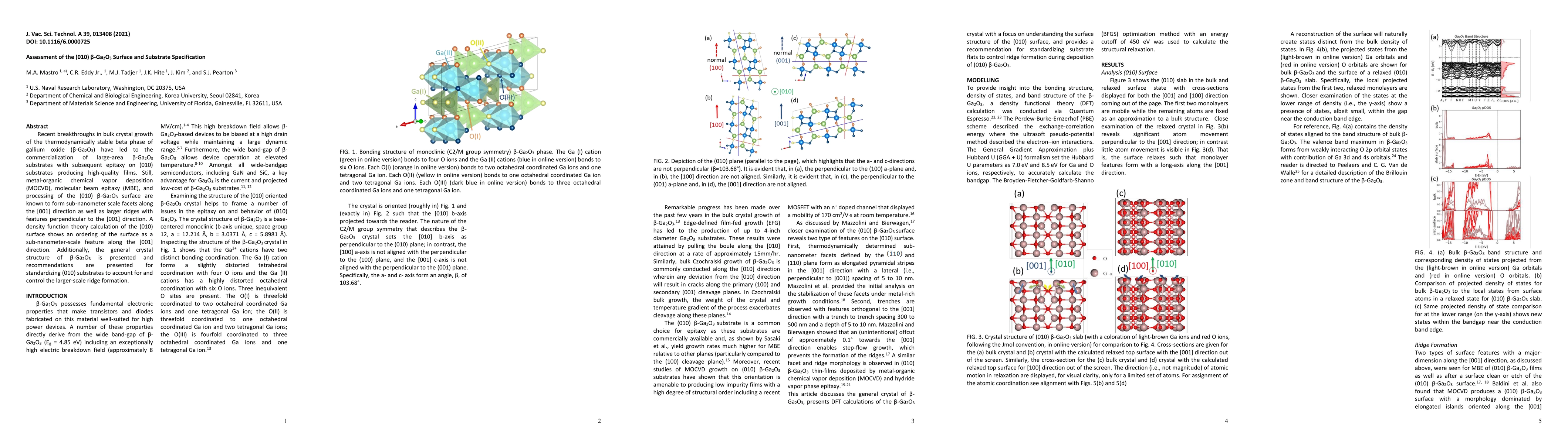
Recent breakthroughs in bulk crystal growth of the thermodynamically stable beta phase of gallium oxide ($\beta$-Ga$_2$O$_3$) have led to the commercialization of large-area beta-Ga$_2$O$_3$ substra...
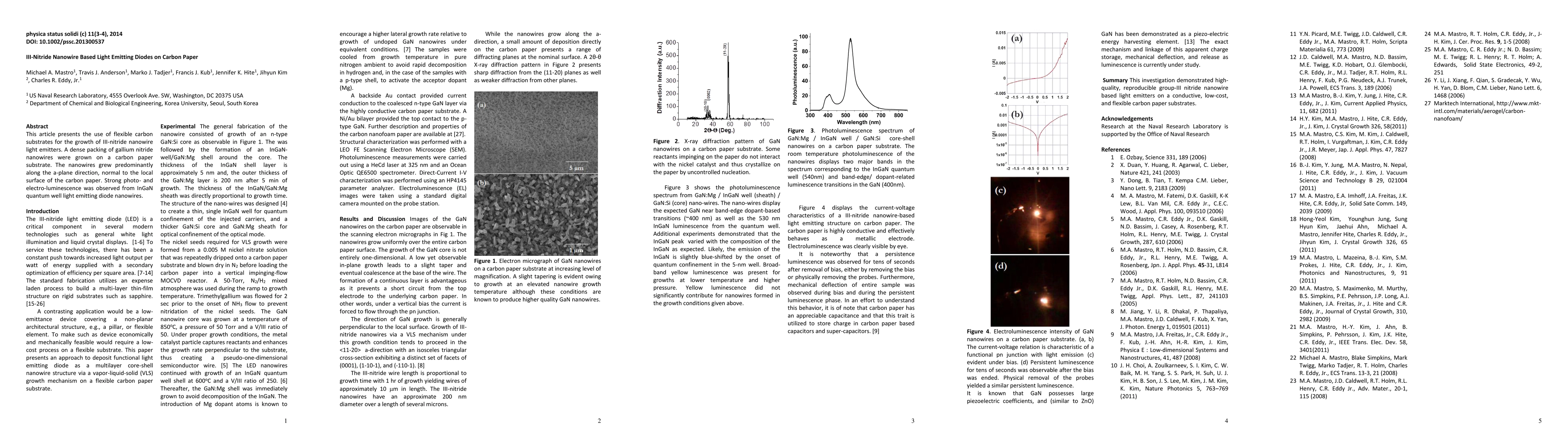
This article presents the use of flexible carbon substrates for the growth of III-nitride nanowire light emitters. A dense packing of gallium nitride nanowires were grown on a carbon paper substrate...
Ga2O3 has attracted great attention for electronic device applications due to its ultra-wide bandgap, high breakdown electric field, and large-area affordable substrates grown from the melt. However...
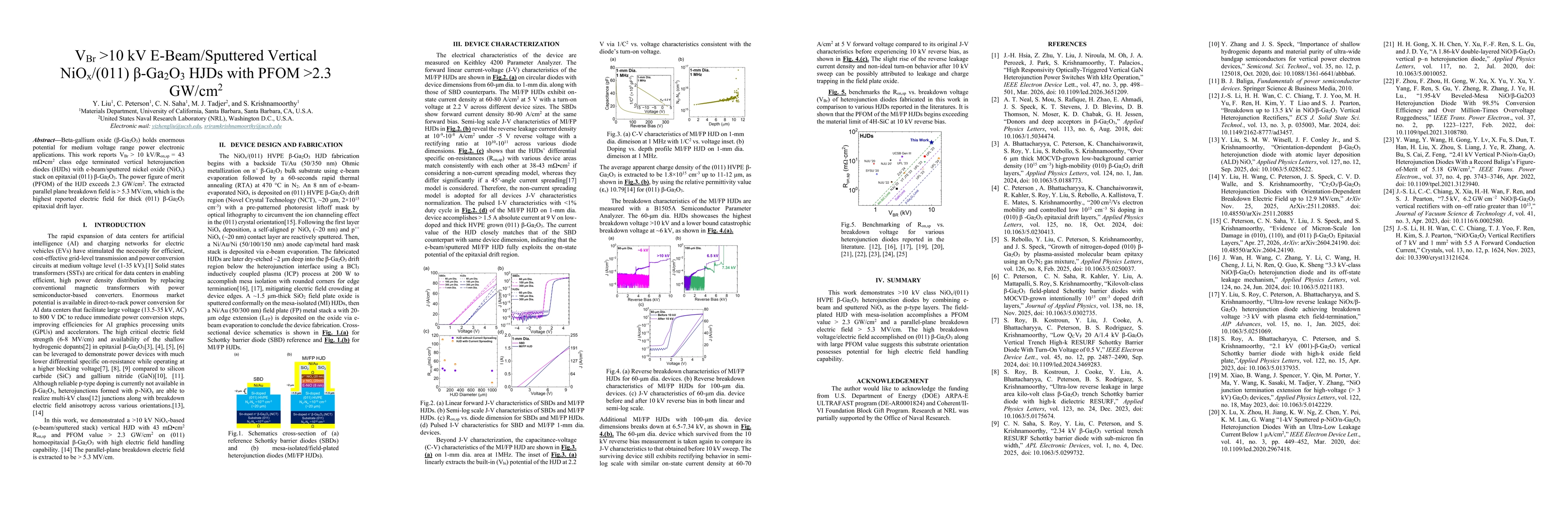
Beta-gallium oxide (β-Ga2O3) holds enormous potential for medium voltage range power electronic applications. This work reports VBr > 10 kV/Ron,sp = 43 mΩ*cm2 class edge terminated vertical heterojunc...
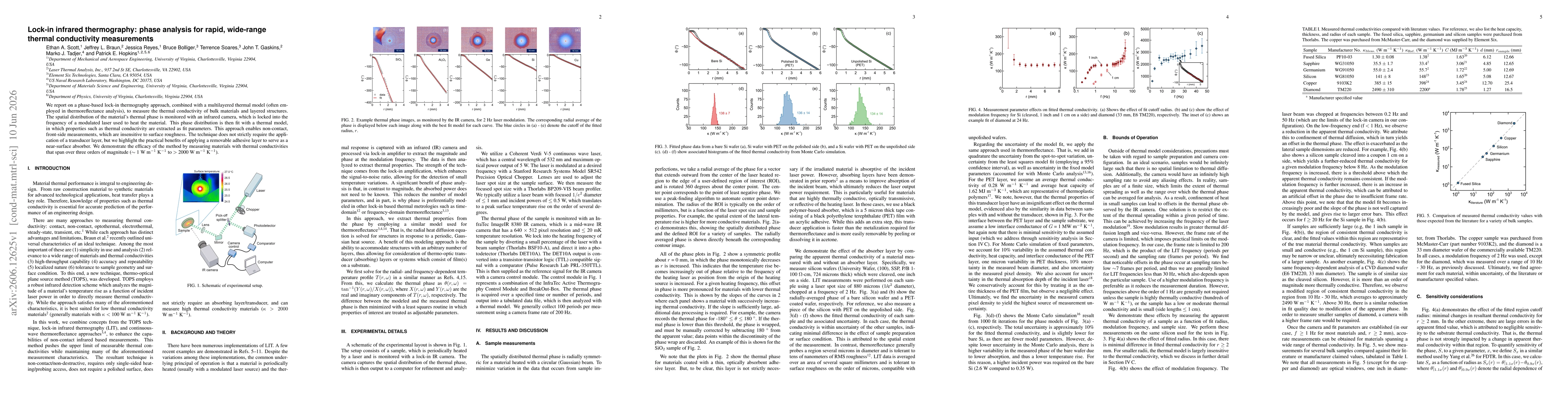
We report on a phase-based lock-in thermography approach, combined with a multilayered thermal model (often employed in thermoreflectance analysis), to measure the thermal conductivity of bulk materia...