Academic Profile
Statistics
Similar Authors
Papers on arXiv
The fields of machine learning and artificial intelligence drive researchers to explore energy-efficient, brain-inspired new hardware. Reservoir computing encompasses recurrent neural networks for s...
Plasmonic refractive index sensors are essential for detecting subtle variations in the ambient environment through surface plasmon interactions. Current efforts utilizing CMOS-compatible, plasmo-ph...
The clock speed of electronic circuits has been stagnant at a few gigahertz for almost two decades because of the breakdown of Dennard scaling, which states that by shrinking the size of transistors...
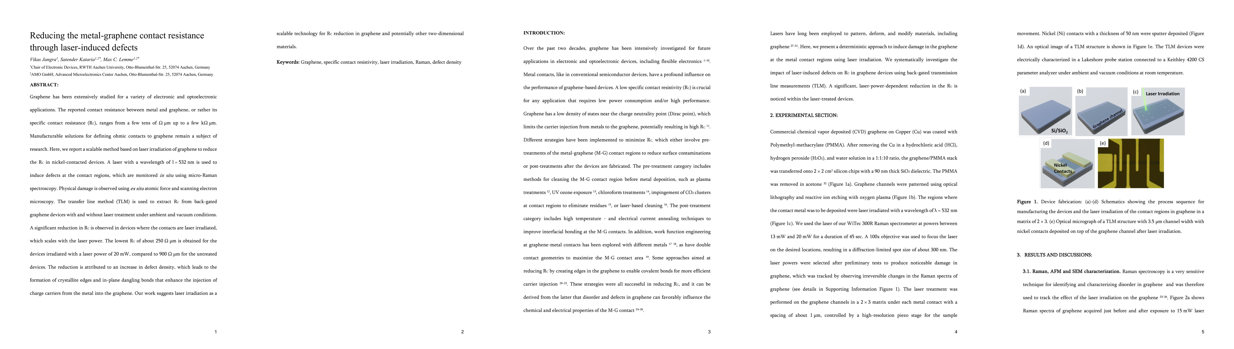
Graphene has been extensively studied for a variety of electronic and optoelectronic applications. The reported contact resistance between metal and graphene, or rather its specific contact resistan...
Two-dimensional (2D) materials are popular candidates for emerging nanoscale devices, including memristors. Resistive switching (RS) in such 2D material memristors has been attributed to the formati...
Graphene is a promising material for applications as a channel in graphene field-effect transistors (GFETs) which may be used as a building block for optoelectronics, high-frequency devices and sens...
Two-dimensional (2D) materials are considered for numerous applications in microelectronics, although several challenges remain when integrating them into functional devices. Weak adhesion is one of...
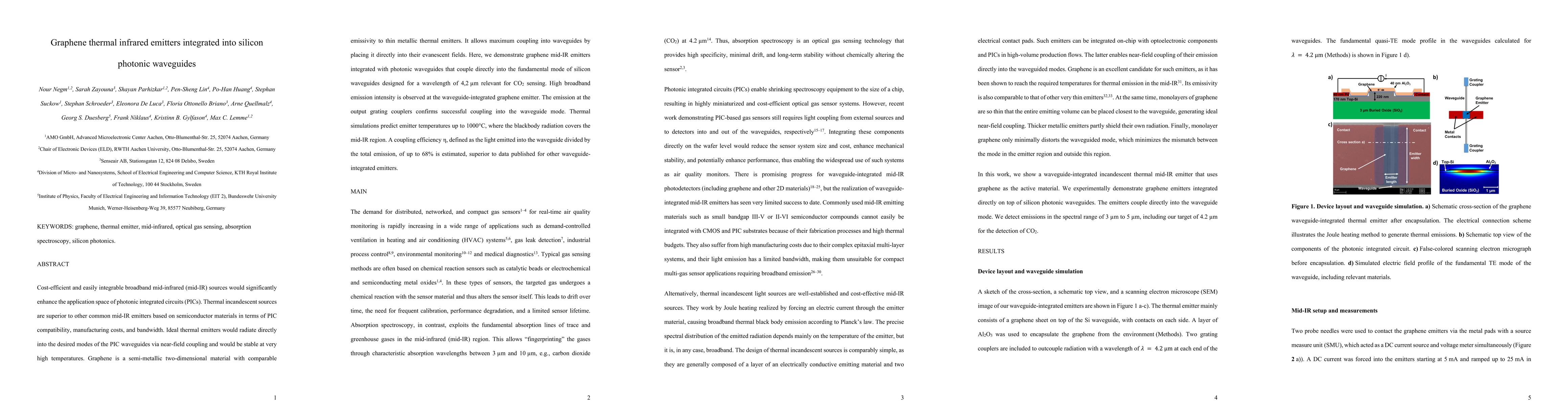
Cost-efficient and easily integrable broadband mid-infrared (mid-IR) sources would significantly enhance the application space of photonic integrated circuits (PICs). Thermal incandescent sources ar...
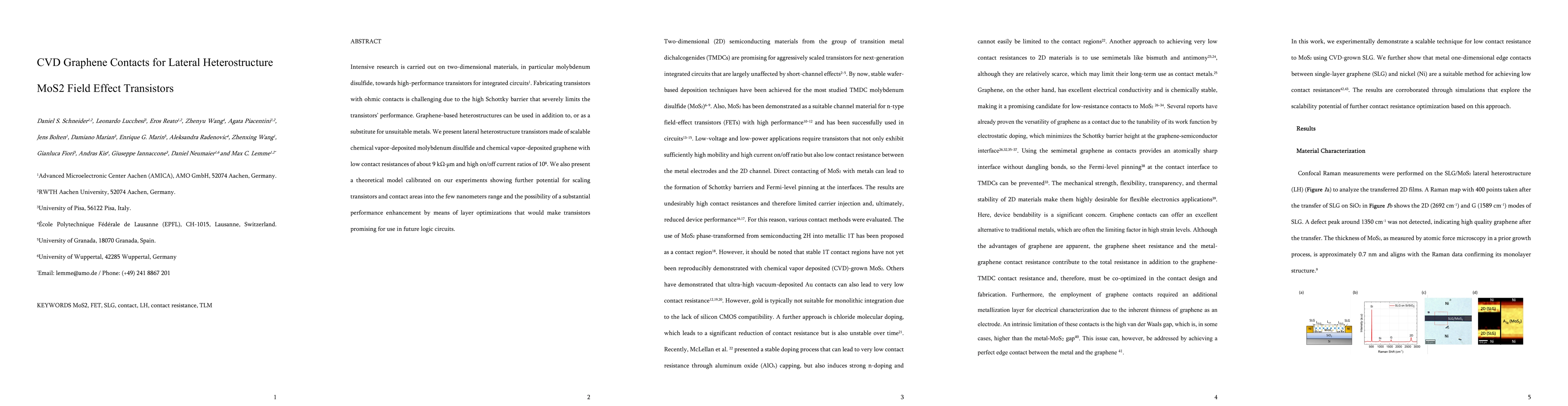
Intensive research is carried out on two-dimensional materials, in particular molybdenum disulfide, towards high-performance transistors for integrated circuits. Fabricating transistors with ohmic c...
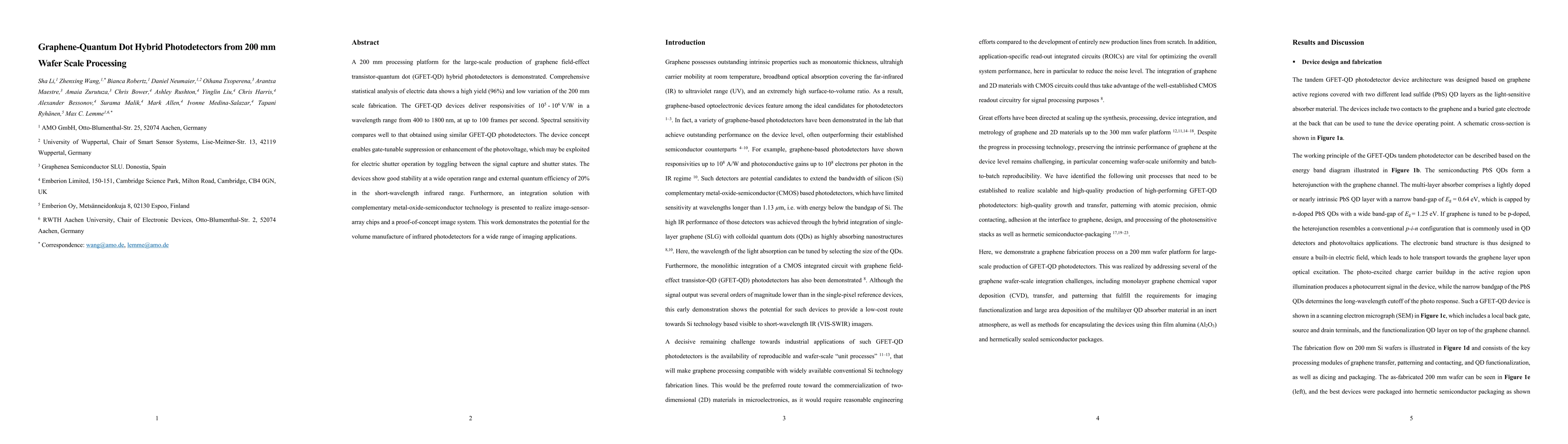
A 200 mm processing platform for the large-scale production of graphene field-effect transistor-quantum dot (GFET-QD) hybrid photodetectors is demonstrated. Comprehensive statistical analysis of ele...
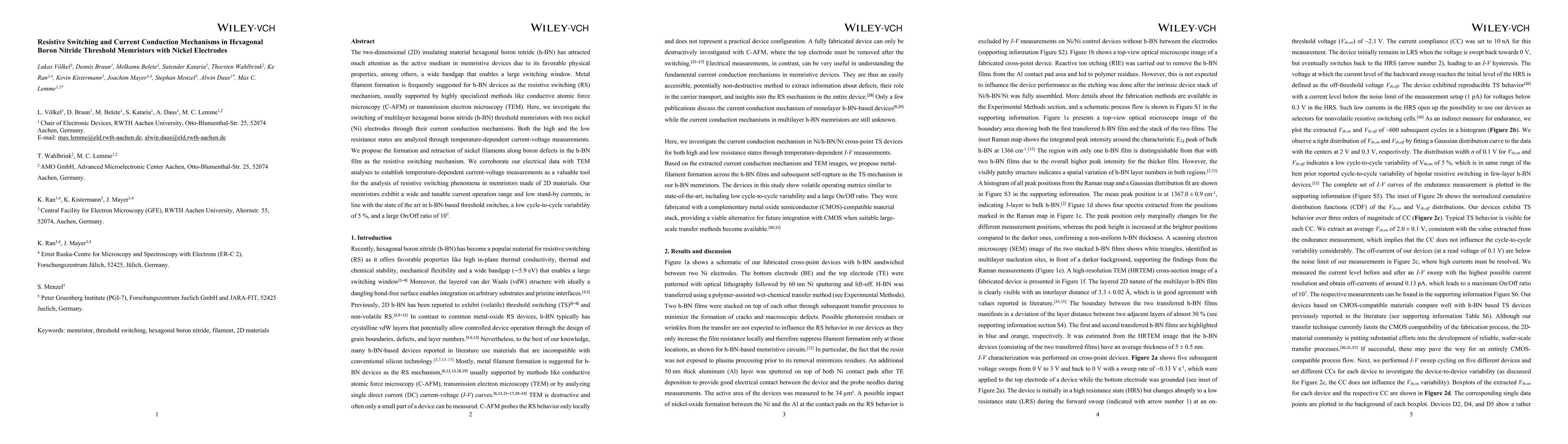
The two-dimensional (2D) insulating material hexagonal boron nitride (h BN) has attracted much attention as the active medium in memristive devices due to its favorable physical properties, among ot...

Titanium dioxide (TiO$_2$) thin films are commonly used as photocatalytic materials. Here, we enhance the photocatalytic activity of devices based on TiO$_2$ by combining nanostructured glass substr...
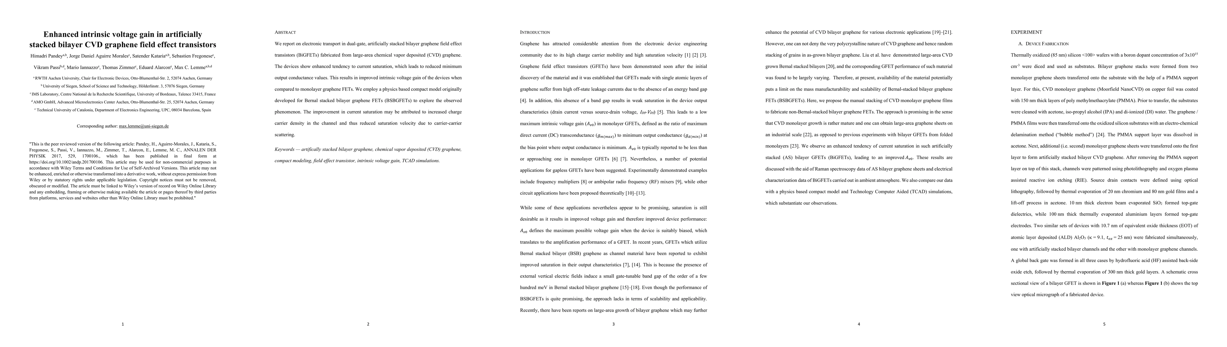
We report on electronic transport in dual-gate, artificially stacked bilayer graphene field effect transistors (BiGFETs) fabricated from large-area chemical vapor deposited (CVD) graphene. The devic...
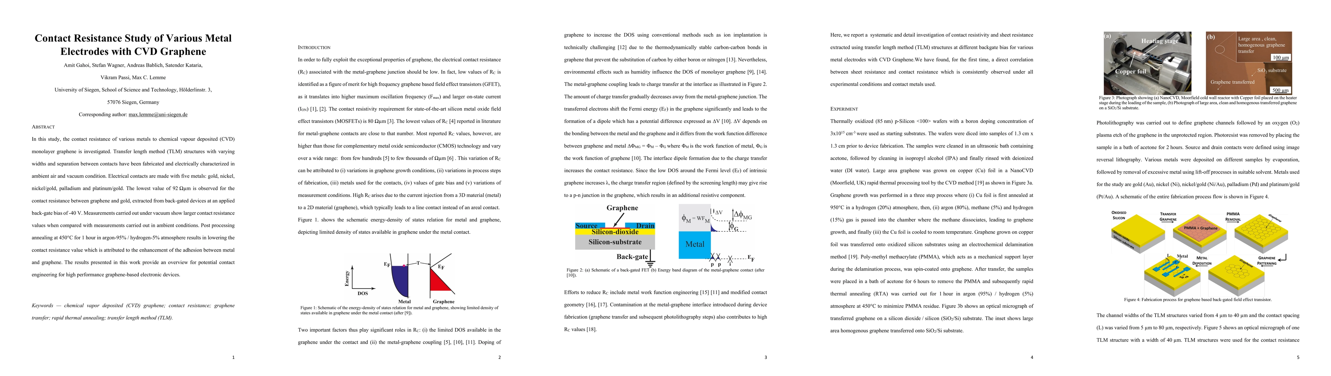
In this study, the contact resistance of various metals to chemical vapour deposited (CVD) monolayer graphene is investigated. Transfer length method (TLM) structures with varying widths and separat...
Laser resonators have outputs with Gaussian spatial beam profiles. In laser interference lithography (LIL), using such Gaussian shaped beams leads to an inhomogeneous exposure of the substrate. As a...
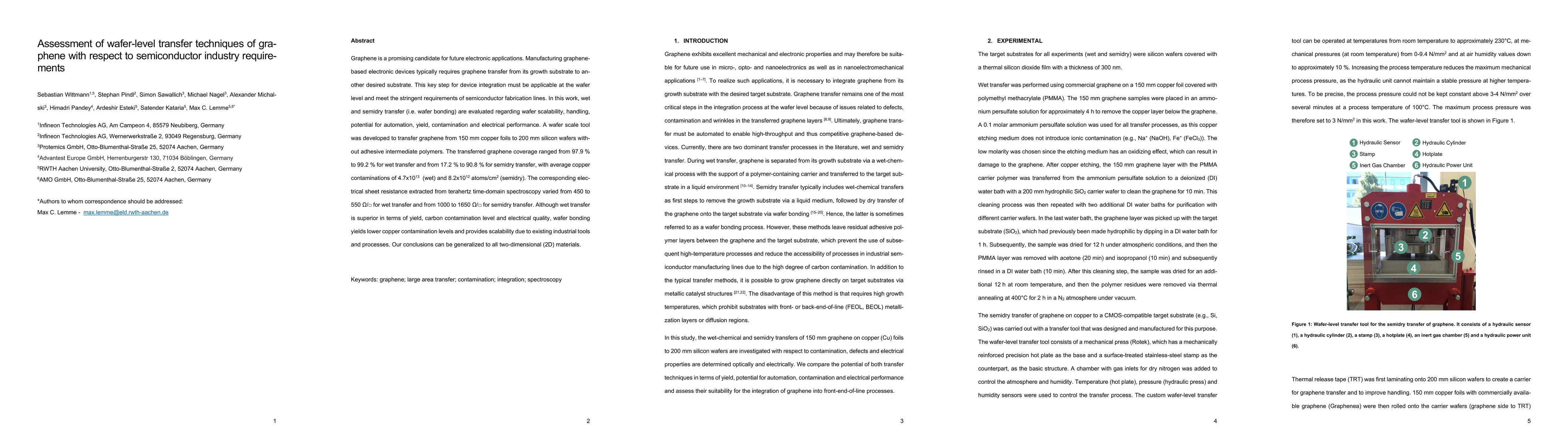
Graphene is a promising candidate for future electronic applications. Manufacturing graphene-based electronic devices typically requires graphene transfer from its growth substrate to another desire...
The deposition of dielectric materials on graphene is one of the bottlenecks for unlocking the potential of graphene in electronic applications. In this paper we demonstrate the plasma enhanced atom...
Particle contamination of extreme ultraviolet (EUV) photomasks is one of the numerous challenges in nanoscale semiconductor fabrication, since it can lead to systematic device failures when disturbe...
Electrochemically exfoliated graphene (e-G) thin films on Nafion$^{(R)}$ membranes exhibit a selective barrier effect against undesirable fuel crossover. The approach combines the high proton conduc...
Two-dimensional (2D) materials, such as graphene, are seen as potential candidates for fabricating electronic devices and circuits on flexible substrates. Inks or dispersions of 2D materials can be ...
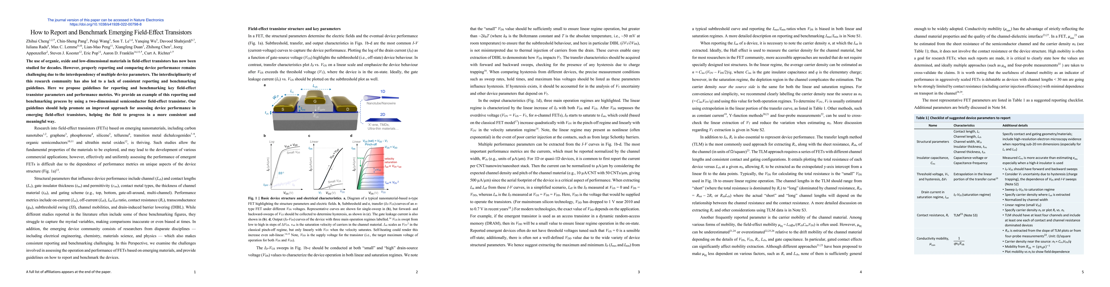
Emerging low-dimensional nanomaterials have been studied for decades in device applications as field-effect transistors (FETs). However, properly reporting and comparing device performance has been ...
We demonstrate the design, fabrication, and characterization of wafer-scale, zero-bias power detectors based on two-dimensional MoS$_2$ field effect transistors (FETs). The MoS$_2$ FETs are fabricat...
PtSe$_2$ is one of the most promising materials for the next generation of piezoresistive sensors. However, the large-scale synthesis of homogeneous thin films with reproducible electromechanical pr...
Low cost, easily integrable photodetectors (PDs) for silicon (Si) photonics are still a bottleneck for photonic integrated circuits (PICs), especially for wavelengths above 1.8 ${\mu}$m. Multilayere...
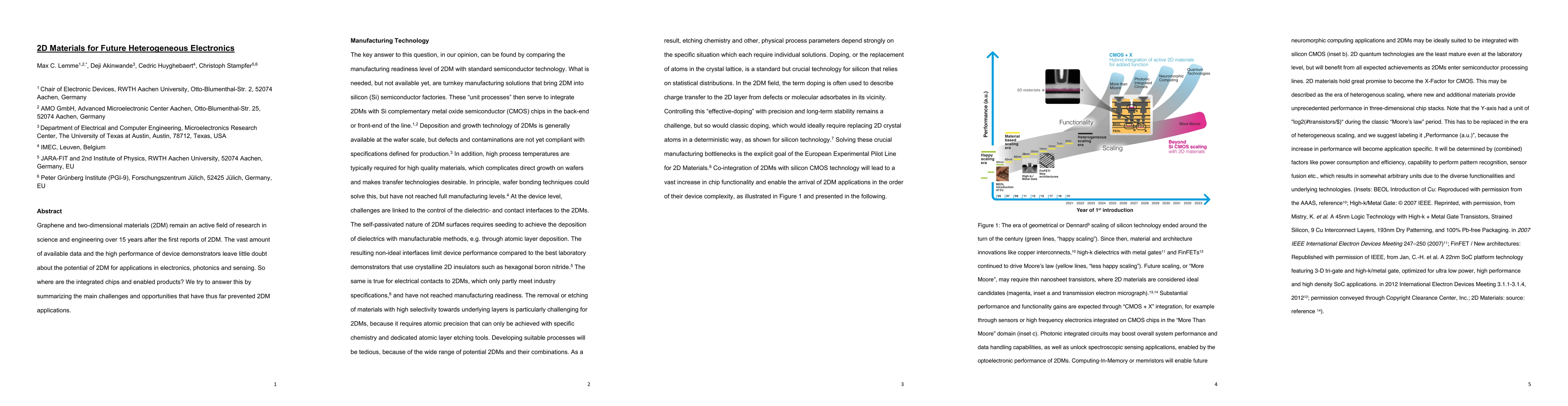
Graphene and two-dimensional materials (2DM) remain an active field of research in science and engineering over 15 years after the first reports of 2DM. The vast amount of available data and the hig...
Flexible energy harvesting devices fabricated in scalable thin-film processes are important components in the field of wearable electronics and the Internet of Things. We present a flexible rectenna...
Despite the enormous progress achieved during the past decade, nanoelectronic devices based on two-dimensional (2D) semiconductors still suffer from a limited electrical stability. This limited stab...
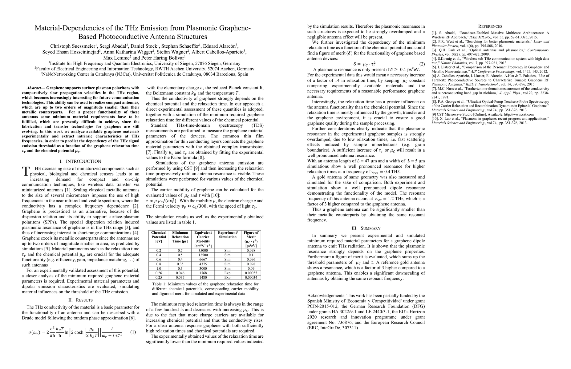
Graphene supports surface plasmon polaritons with comparatively slow propagation velocities in the THz region, which becomes increasingly interesting for future communication technologies. This abil...
Platinum diselenide (PtSe${_2}$) is a two-dimensional (2D) material with outstanding electronic and piezoresistive properties. The material can be grown at low temperatures in a scalable manner whic...
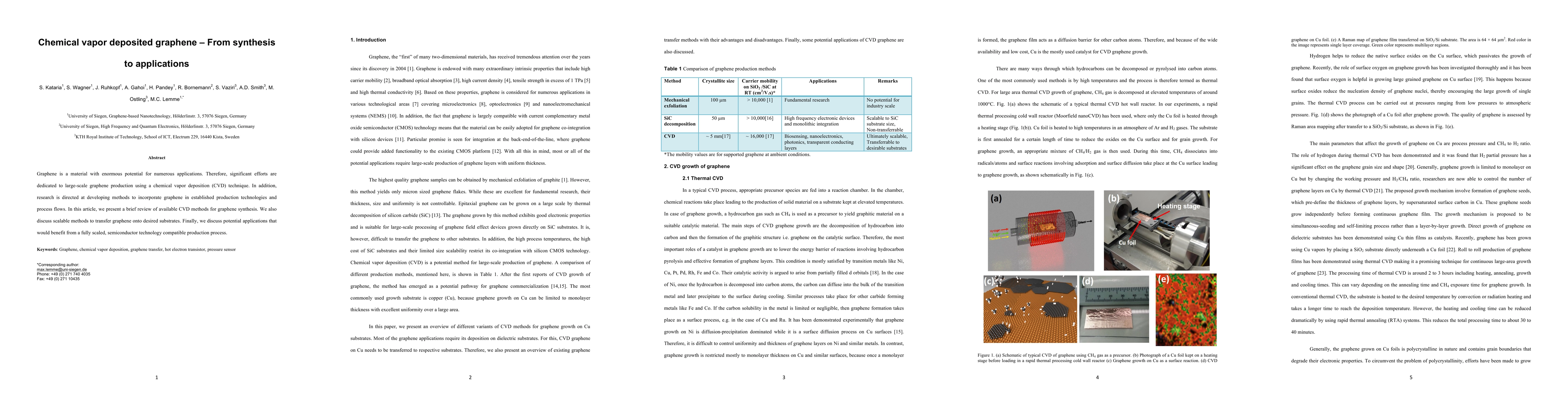
Graphene is a material with enormous potential for numerous applications. Therefore, significant efforts are dedicated to large-scale graphene production using a chemical vapor deposition (CVD) tech...
Diodes made of heterostructures of the 2D material graphene and conventional 3D materials are reviewed in this manuscript. Several applications in high frequency electronics and optoelectronics are ...
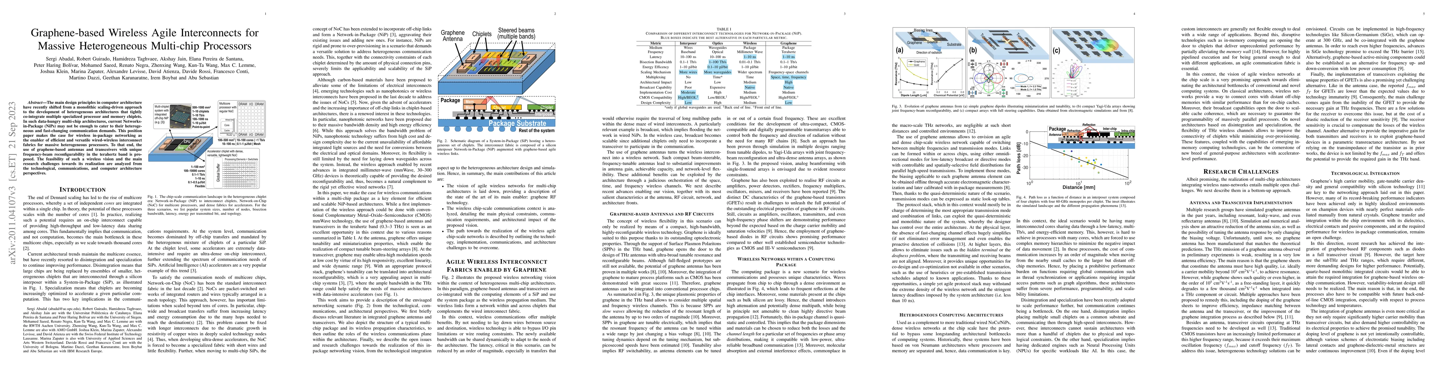
The main design principles in computer architecture have recently shifted from a monolithic scaling-driven approach to the development of heterogeneous architectures that tightly co-integrate multip...
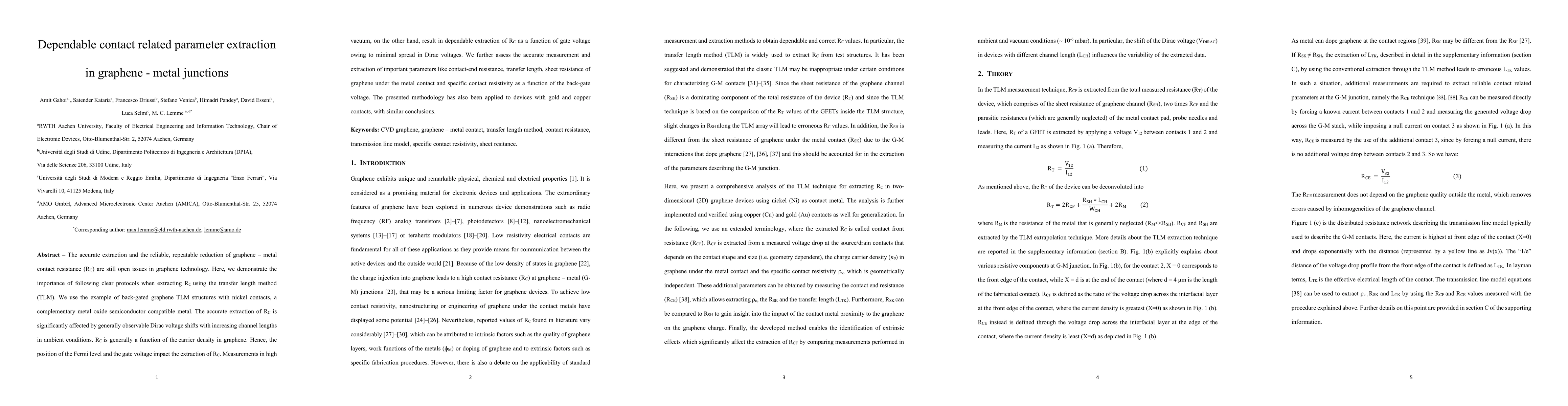
The accurate extraction and the reliable, repeatable reduction of graphene - metal contact resistance (R$_{C}$) are still open issues in graphene technology. Here, we demonstrate the importance of f...
The unique properties and atomic thickness of two-dimensional (2D) materials enable smaller and better nanoelectromechanical sensors with novel functionalities. During the last decade, many studies ...
Graphene is an atomically thin material that features unique electrical and mechanical properties, which makes it an extremely promising material for future nanoelectromechanical systems (NEMS). Rec...
Unparalleled strength, chemical stability, ultimate surface-to-volume ratio and excellent electronic properties of graphene make it an ideal candidate as a material for membranes in micro- and nanoe...
Nanoelectromechanical system (NEMS) sensors and actuators could be of use in the development of next generation mobile, wearable, and implantable devices. However, these NEMS devices require transdu...
Heterostructures comprising of silicon (Si), molybdenum disulfide (MoS${_2}$) and graphene are investigated with respect to the vertical current conduction mechanism. The measured current-voltage (I...
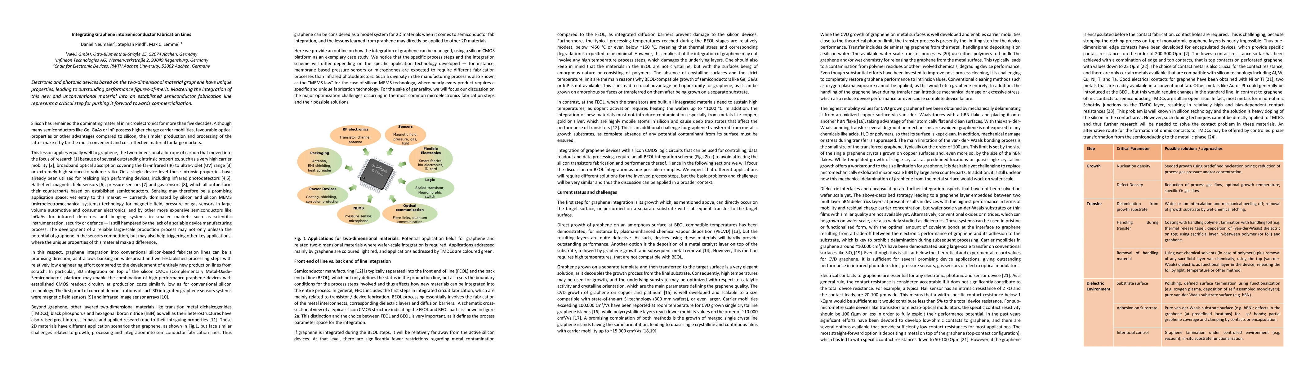
Electronic and photonic devices based on the two-dimensional material graphene have unique properties, leading to outstanding performance figures-of-merit. Mastering the integration of this new and ...

Non-volatile resistive switching is demonstrated in memristors with nanocrystalline molybdenum disulfide (MoS$_2$) as the active material. The vertical heterostructures consist of silicon, verticall...
We demonstrate a novel concept for operating graphene-based Hall sensors using an alternating current (AC) modulated gate voltage, which provides three important advantages compared to Hall sensors ...
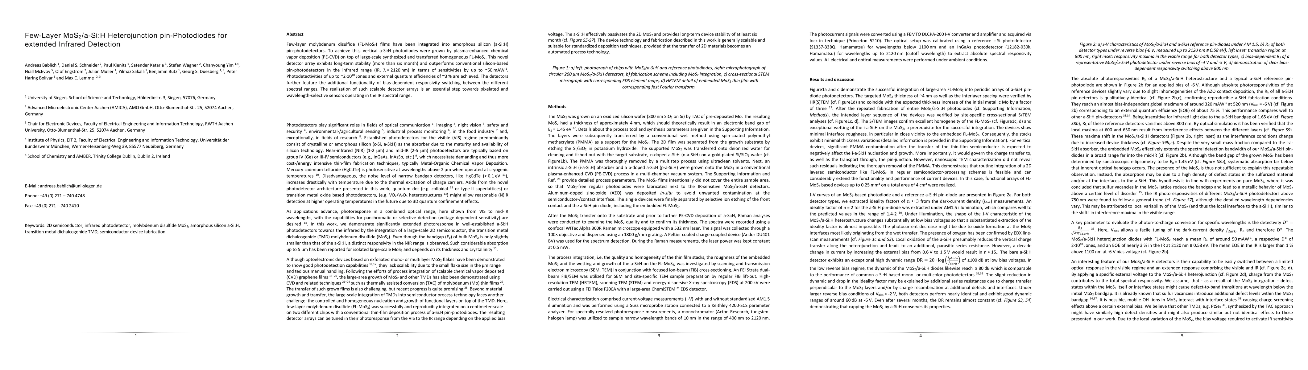
Few-layer molybdenum disulfide (FL-MoS$_2$) films have been integrated into amorphous silicon (a-Si:H) pin photodetectors. To achieve this, vertical a-Si:H photodiodes were grown by plasma-enhanced ...
A systematic investigation of graphene edge contacts is provided. Intentionally patterning monolayer graphene at the contact region creates well-defined edge contacts that lead to a 67% enhancement ...
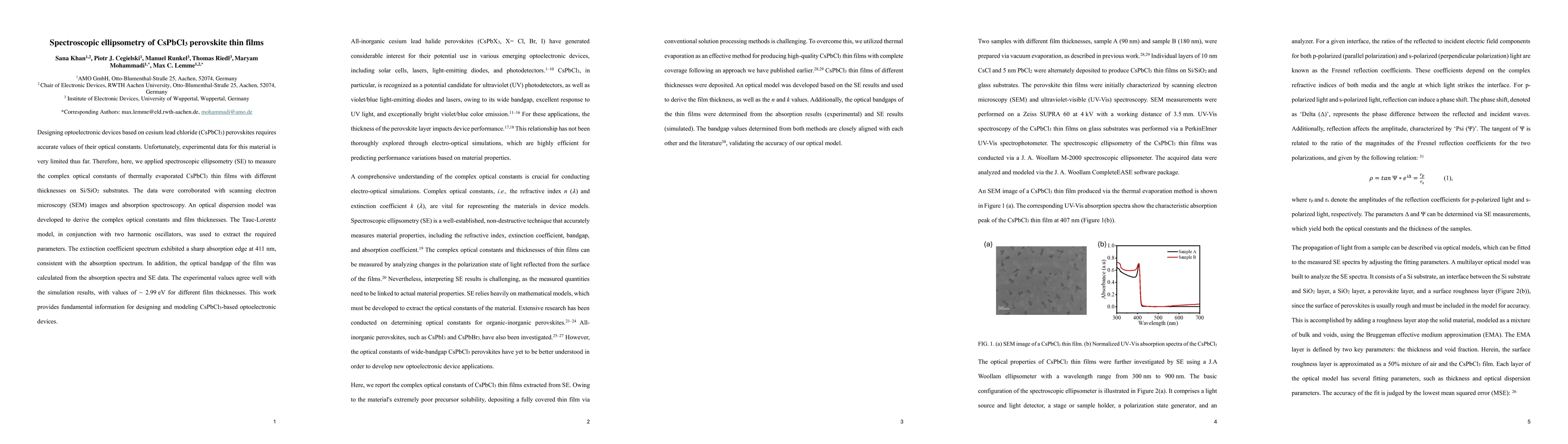
Designing optoelectronic devices based on cesium lead chloride (CsPbCl${_3}$) perovskites requires accurate values of their optical constants. Unfortunately, experimental data for this material is ver...
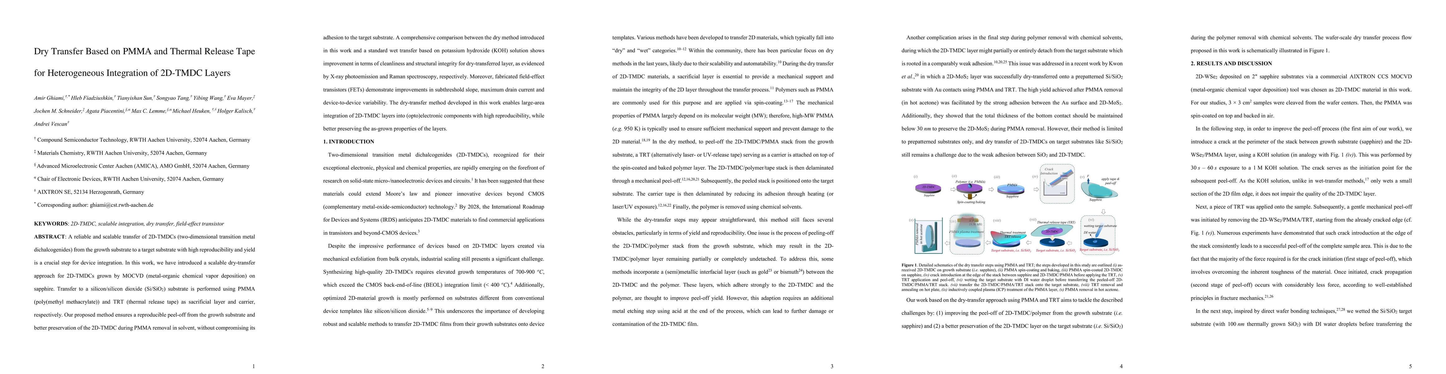
A reliable and scalable transfer of 2D-TMDCs (two-dimensional transition metal dichalcogenides) from the growth substrate to a target substrate with high reproducibility and yield is a crucial step fo...
Graphene is being increasingly used as an interesting transducer membrane in micro- and nanoelectromechanical systems (MEMS and NEMS, respectively) due to its atomical thickness, extremely high carrie...
Metal-halide perovskites (MHPs) have exciting optoelectronic properties and are under investigation for various applications, such as photovoltaics, light-emitting diodes, and lasers. An essential ste...
Layered two-dimensional (2D) semiconductors have shown enhanced ion migration capabilities along their van der Waals (vdW) gaps and on their surfaces. This effect can be employed for resistive switchi...
Two-dimensional materials (2DMs) have been widely investigated because of their potential for heterogeneous integration with modern electronics. However, several major challenges remain, such as the d...

Membrane-based sensors are an important market for microelectromechanical systems (MEMS). Two-dimensional (2D) materials, with their low mass, are excellent candidates for suspended membranes to provi...

Suspended membranes of monoatomic graphene exhibit great potential for applications in electronic and nanoelectromechanical devices. In this work, a "hot and dry" transfer process is demonstrated to a...
A method for assessing the quality of electronic material properties of thin-film metal oxide semiconductor field-effect transistors (MOSFETs) is presented. By investigating samples with MOCVD-grown M...
Two-dimensional material (2DM)-based field-effect transistors (FETs), such as molybdenum disulfide (MoS${_2}$)-FETs, have gained significant attention for their potential for ultra-short channels, the...
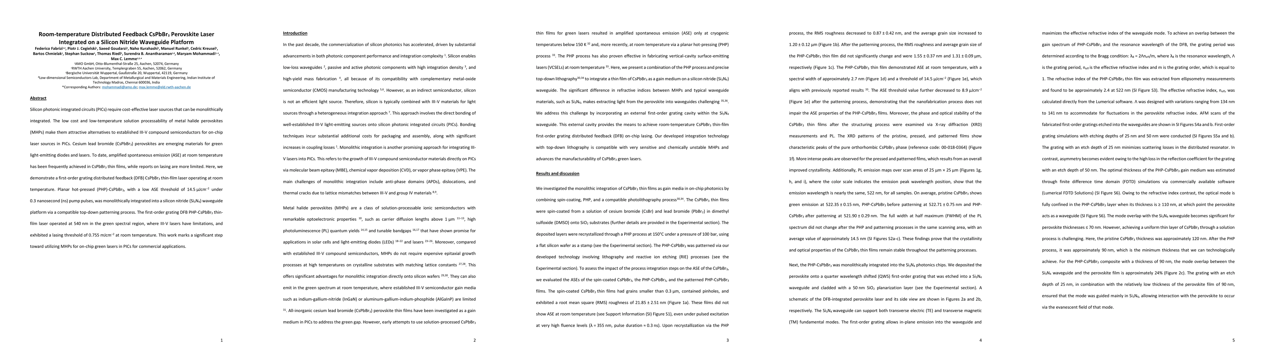
Silicon photonic integrated circuits (PICs) require cost-effective laser sources that can be monolithically integrated. The low cost and low-temperature solution processability of metal halide perovsk...
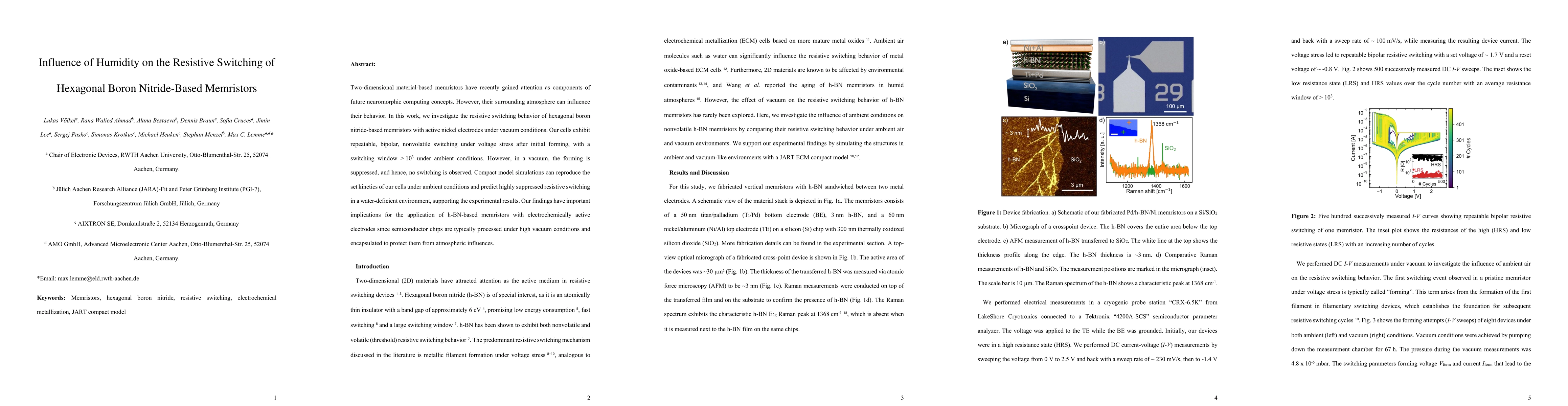
Two-dimensional material-based memristors have recently gained attention as components of future neuromorphic computing concepts. However, their surrounding atmosphere can influence their behavior. In...
Threshold switching (TS) is a phenomenon where non-permanent changes in electrical resistance of a two-terminal device can be controlled by modulating the voltage bias. TS based on silver (Ag) conduct...
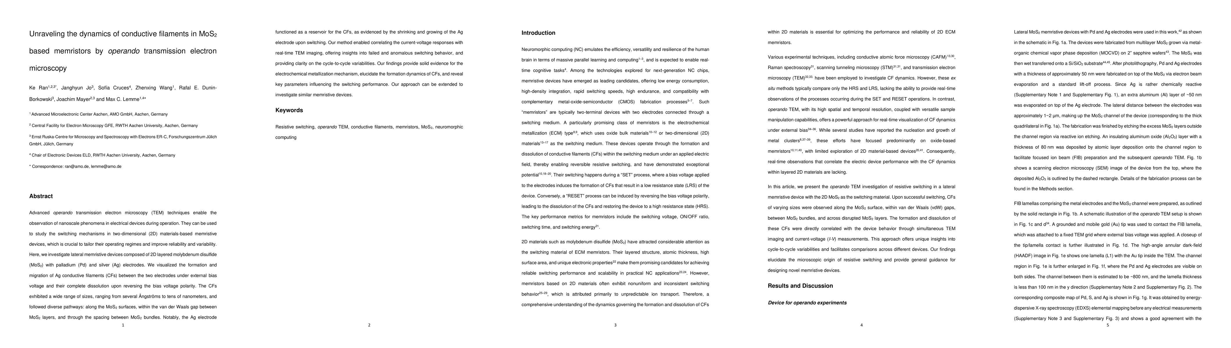
Advanced operando transmission electron microscopy (TEM) techniques enable the observation of nanoscale phenomena in electrical devices during operation. They can be used to study the switching mechan...
Developing electronic devices capable of emulating biological functions is essential for advancing brain-inspired computation paradigms such as neuromorphic computing. In recent years, two-dimensional...
Silver phenylselenide (AgSePh), known as mithrene, is a two-dimensional (2D) organic-inorganic chalcogenide (MOC) semiconductor with a wide direct band gap, narrow blue emission and in-plane anisotrop...
Memristors based on two-dimensional materials (2DMs) have garnered significant attention due to their fast resistive switching (RS) behavior and atomic-level thickness, which enables low power consump...
Layered two-dimensional (2D) materials provide unique structural features, such as physical gaps between their layers that are only connected through van der Waals (vdW) forces. These vdW gaps can gui...
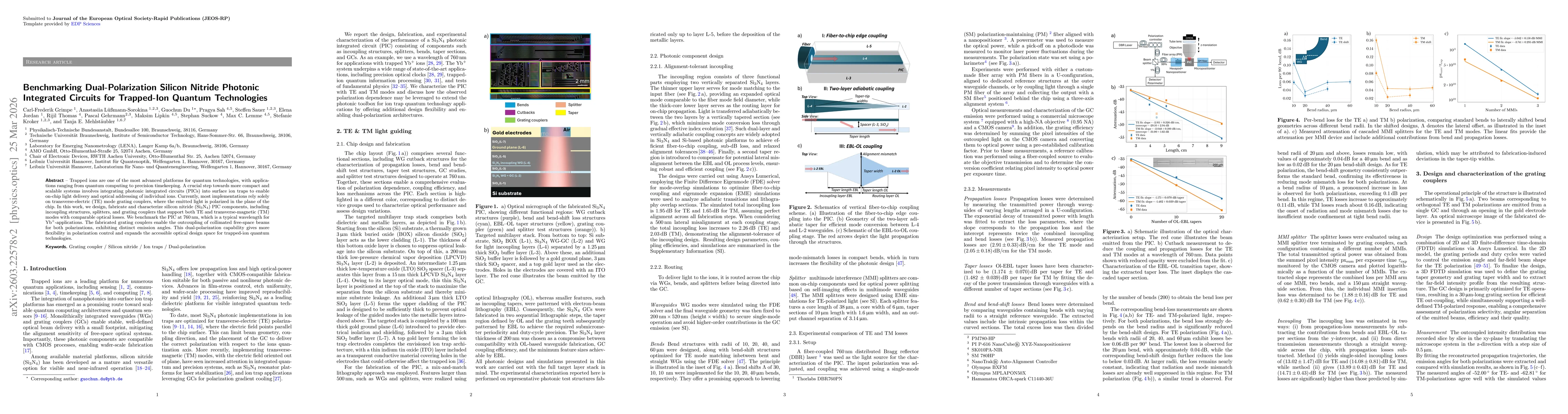
Trapped ions are one of the most advanced platforms for quantum technologies, with applications ranging from quantum computing to precision timekeeping. A crucial step towards more compact and scalabl...
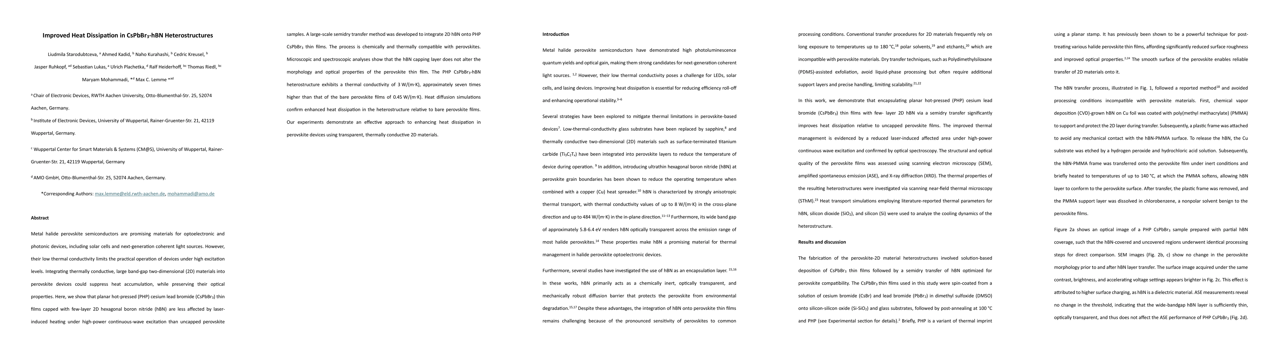
Metal halide perovskite semiconductors are promising materials for optoelectronic and photonic devices, including solar cells and next-generation coherent light sources. However, their low thermal con...