01
MethodologyHow they did it
A laser-induced defecting technique was used to create defects in graphene.
This paper presents a scalable method using laser irradiation to reduce the specific contact resistance (R{_C}) between nickel and graphene, achieving a significant reduction to about 250 {\Omega} {\mu}m with 20 mW laser power. The laser-induced defects enhance charge carrier injection, suggesting a viable approach for improving graphene-metal contacts.
A laser-induced defecting technique was used to create defects in graphene. More in Methodology →
The Raman spectra showed a significant increase in D peak intensity at the laser-treated center. — The SEM images revealed physical changes in the graphene channel after laser treatment. More in Key Results →
This research demonstrates a novel method for reducing metal-graphene contact resistance through laser-induced defects. More in Significance →
The laser power and treatment time may not be suitable for all graphene samples. — The technique may not be scalable to larger devices or production lines. More in Limitations →
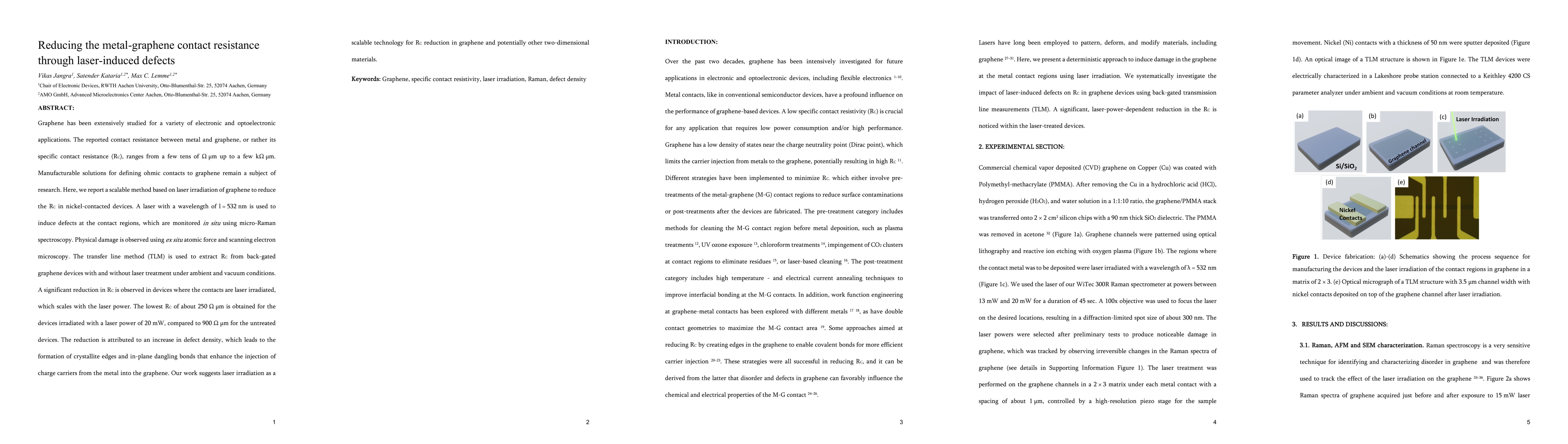
Graphene has been extensively studied for a variety of electronic and optoelectronic applications. The reported contact resistance between metal and graphene, or rather its specific contact resistance (R{_C}), ranges from a few tens of {\Omega} {\mu}m up to a few k{\Omega} {\mu}m. Manufacturable solutions for defining ohmic contacts to graphene remain a subject of research. Here, we report a scalable method based on laser irradiation of graphene to reduce the R{_C} in nickel-contacted devices. A laser with a wavelength of {\lambda} = 532 nm is used to induce defects at the contact regions, which are monitored \textit{in-situ} using micro-Raman spectroscopy. Physical damage is observed using \textit{ex-situ} atomic force and scanning electron microscopy. The transfer line method (TLM) is used to extract R{_C} from back-gated graphene devices with and without laser treatment under ambient and vacuum conditions. A significant reduction in R{_C} is observed in devices where the contacts are laser irradiated, which scales with the laser power. The lowest R{_C} of about 250 {\Omega} {\mu}m is obtained for the devices irradiated with a laser power of 20 mW, compared to 900 {\Omega} {\mu}m for the untreated devices. The reduction is attributed to an increase in defect density, which leads to the formation of crystallite edges and in-plane dangling bonds that enhance the injection of charge carriers from the metal into the graphene. Our work suggests laser irradiation as a scalable technology for R{_C} reduction in graphene and potentially other two-dimensional materials.
Seven facets of this paper, analysed and brought into focus by AI.
This research demonstrates a novel method for reducing metal-graphene contact resistance through laser-induced defects.
A laser-induced defecting technique was used to create defects in graphene.
This research demonstrates a novel method for reducing metal-graphene contact resistance through laser-induced defects.
A new method for reducing metal-graphene contact resistance through laser-induced defects was developed.
This work introduces a novel approach to improving graphene-metal contact resistance, which is essential for high-performance electronics.
Current paper (gray), citations (green), references (blue)
Display is limited for performance on very large graphs.
Discussion 0