Academic Profile
Statistics
Similar Authors
Papers on arXiv
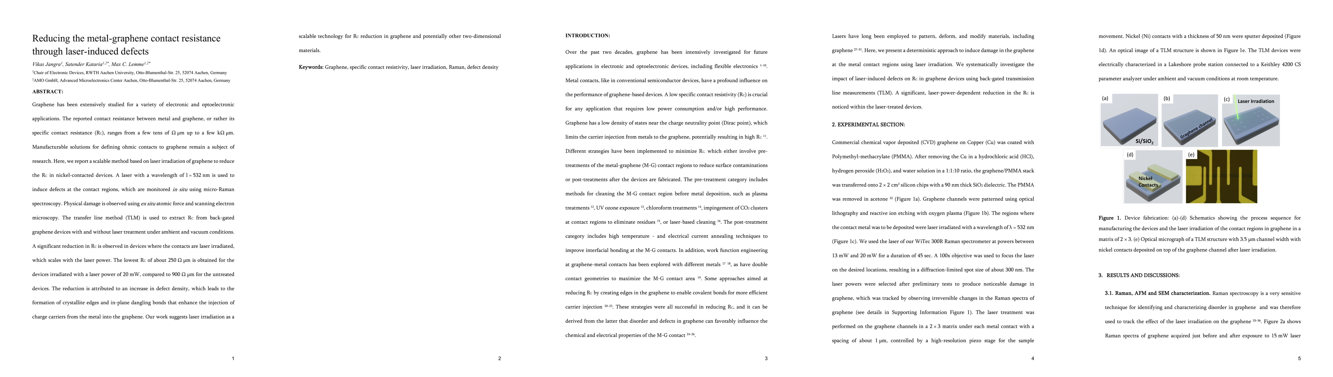
Graphene has been extensively studied for a variety of electronic and optoelectronic applications. The reported contact resistance between metal and graphene, or rather its specific contact resistan...
The two-dimensional (2D) insulating material hexagonal boron nitride (h BN) has attracted much attention as the active medium in memristive devices due to its favorable physical properties, among ot...
We report on electronic transport in dual-gate, artificially stacked bilayer graphene field effect transistors (BiGFETs) fabricated from large-area chemical vapor deposited (CVD) graphene. The devic...
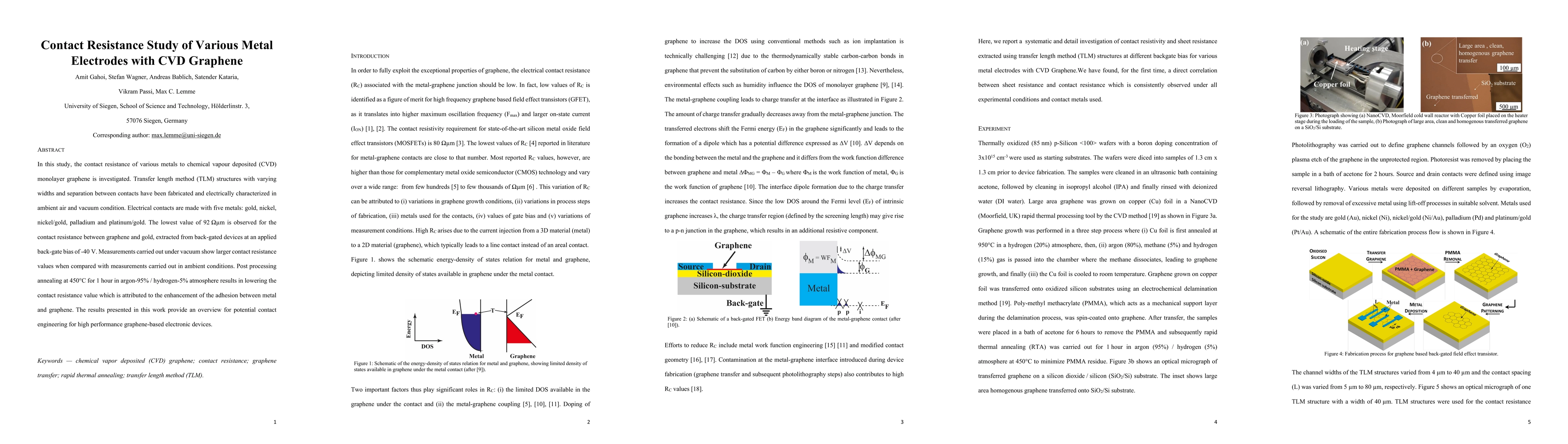
In this study, the contact resistance of various metals to chemical vapour deposited (CVD) monolayer graphene is investigated. Transfer length method (TLM) structures with varying widths and separat...
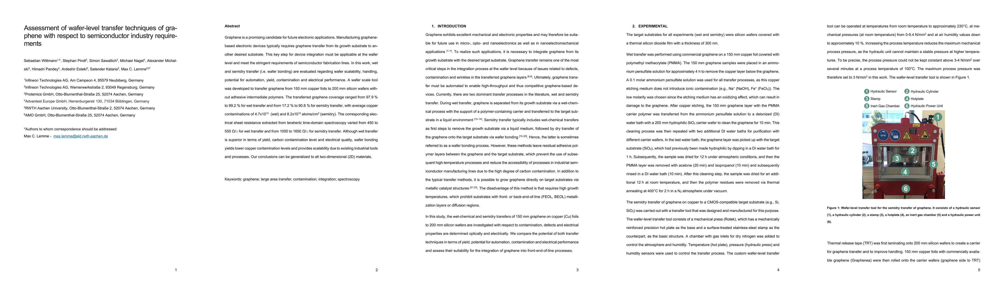
Graphene is a promising candidate for future electronic applications. Manufacturing graphene-based electronic devices typically requires graphene transfer from its growth substrate to another desire...
Two-dimensional (2D) materials, such as graphene, are seen as potential candidates for fabricating electronic devices and circuits on flexible substrates. Inks or dispersions of 2D materials can be ...
Platinum diselenide (PtSe${_2}$) is a two-dimensional (2D) material with outstanding electronic and piezoresistive properties. The material can be grown at low temperatures in a scalable manner whic...
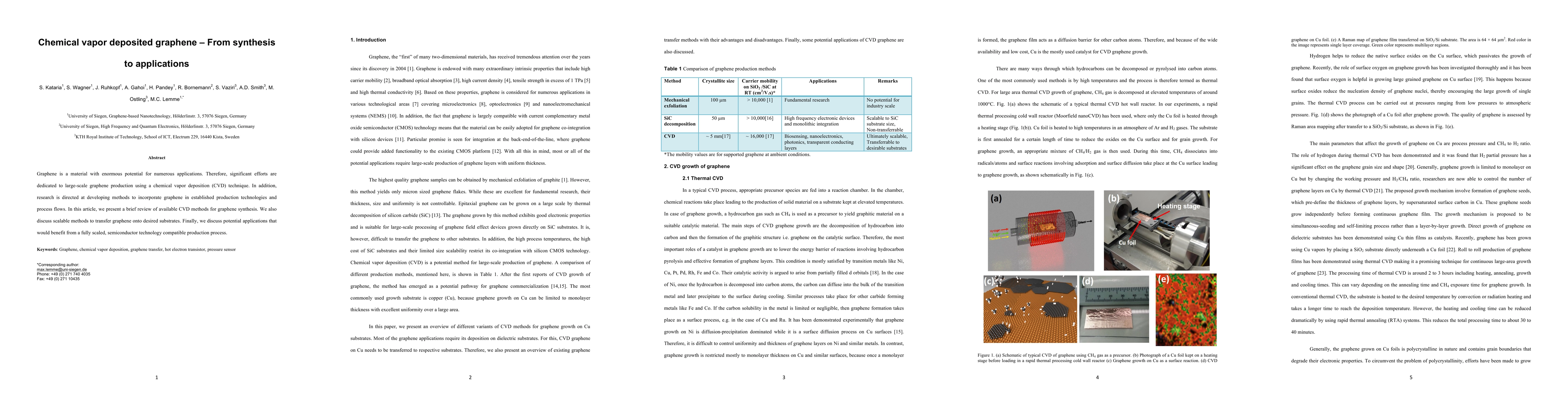
Graphene is a material with enormous potential for numerous applications. Therefore, significant efforts are dedicated to large-scale graphene production using a chemical vapor deposition (CVD) tech...
Diodes made of heterostructures of the 2D material graphene and conventional 3D materials are reviewed in this manuscript. Several applications in high frequency electronics and optoelectronics are ...
The accurate extraction and the reliable, repeatable reduction of graphene - metal contact resistance (R$_{C}$) are still open issues in graphene technology. Here, we demonstrate the importance of f...
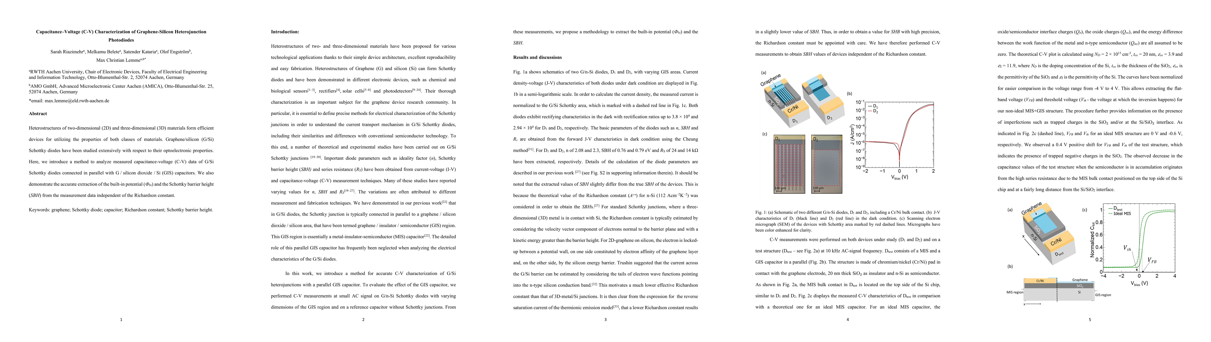
Heterostructures of two-dimensional (2D) and three-dimensional (3D) materials form efficient devices for utilizing the properties of both classes of materials. Graphene/silicon (G/Si) Schottky diode...
Heterostructures comprising of silicon (Si), molybdenum disulfide (MoS${_2}$) and graphene are investigated with respect to the vertical current conduction mechanism. The measured current-voltage (I...

Non-volatile resistive switching is demonstrated in memristors with nanocrystalline molybdenum disulfide (MoS$_2$) as the active material. The vertical heterostructures consist of silicon, verticall...
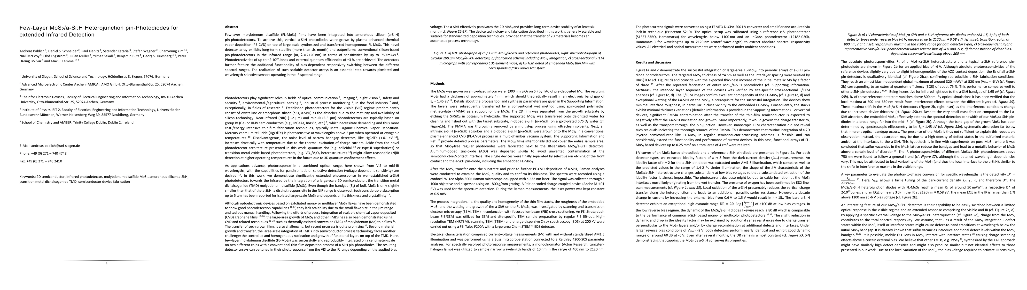
Few-layer molybdenum disulfide (FL-MoS$_2$) films have been integrated into amorphous silicon (a-Si:H) pin photodetectors. To achieve this, vertical a-Si:H photodiodes were grown by plasma-enhanced ...
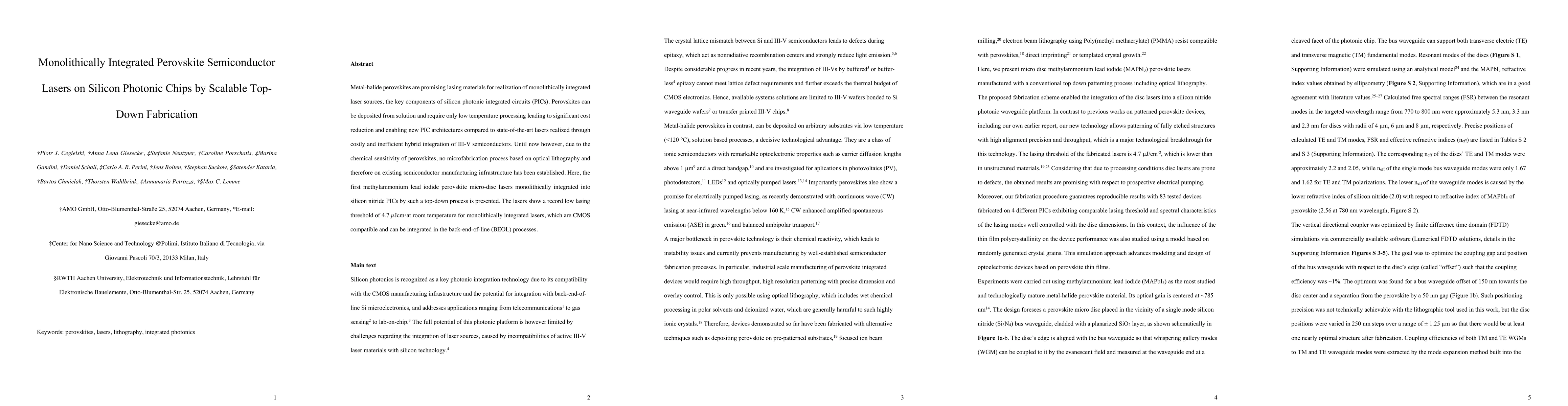
Metal-halide perovskites are promising lasing materials for realization of monolithically integrated laser sources, the key components of silicon photonic integrated circuits (PICs). Perovskites can...
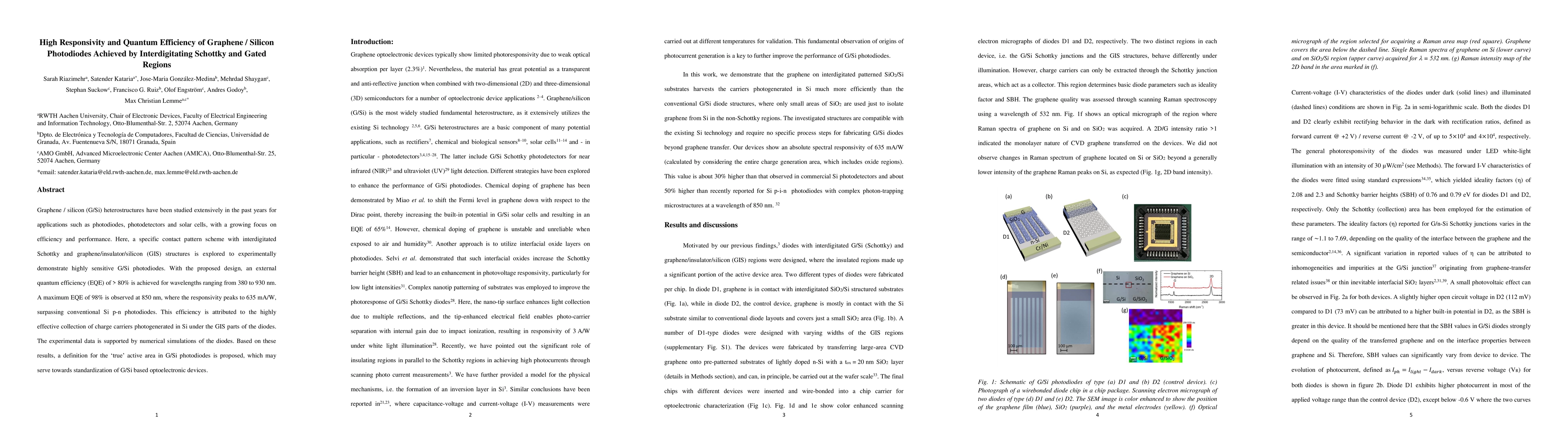
Graphene / silicon (G/Si) heterostructures have been studied extensively in the past years for applications such as photodiodes, photodetectors and solar cells, with a growing focus on efficiency an...