Academic Profile
Statistics
Similar Authors
Papers on arXiv
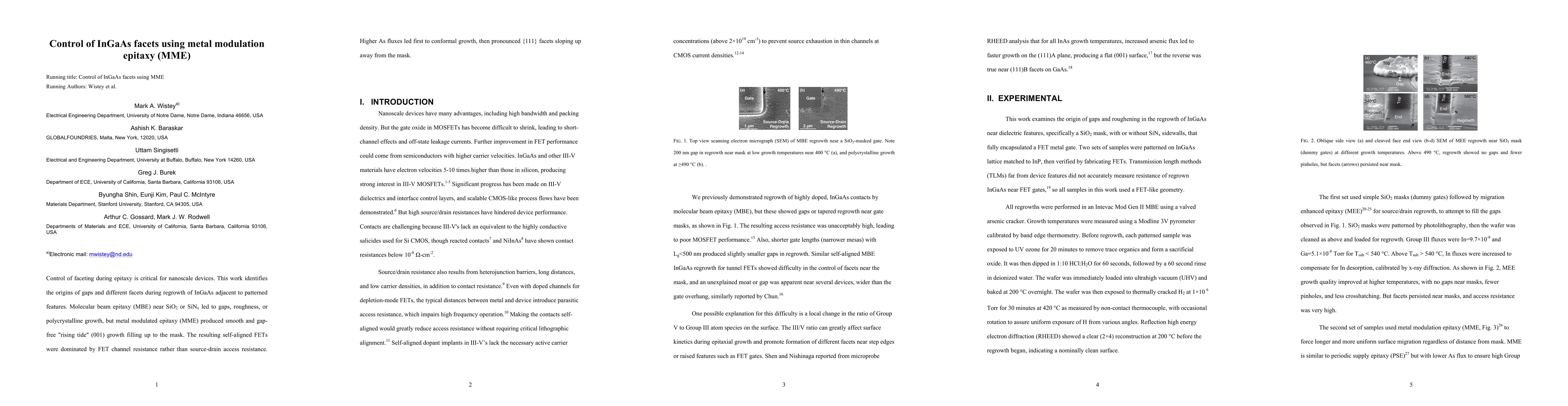
Control of faceting during epitaxy is critical for nanoscale devices. This work identifies the origins of gaps and different facets during regrowth of InGaAs adjacent to patterned features. Molecula...
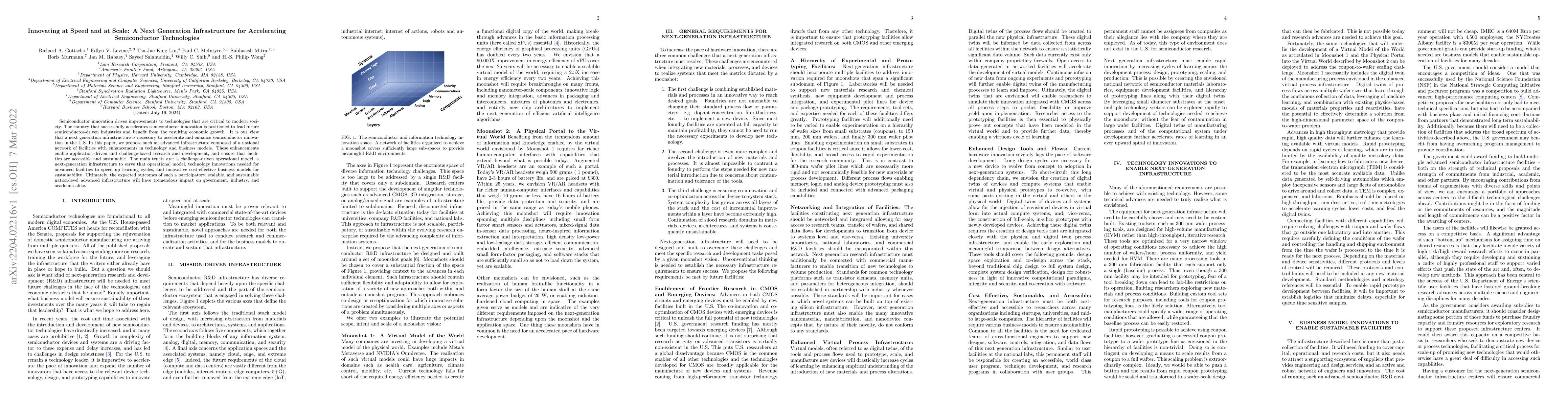
Semiconductor innovation drives improvements to technologies that are critical to modern society. The country that successfully accelerates semiconductor innovation is positioned to lead future semi...
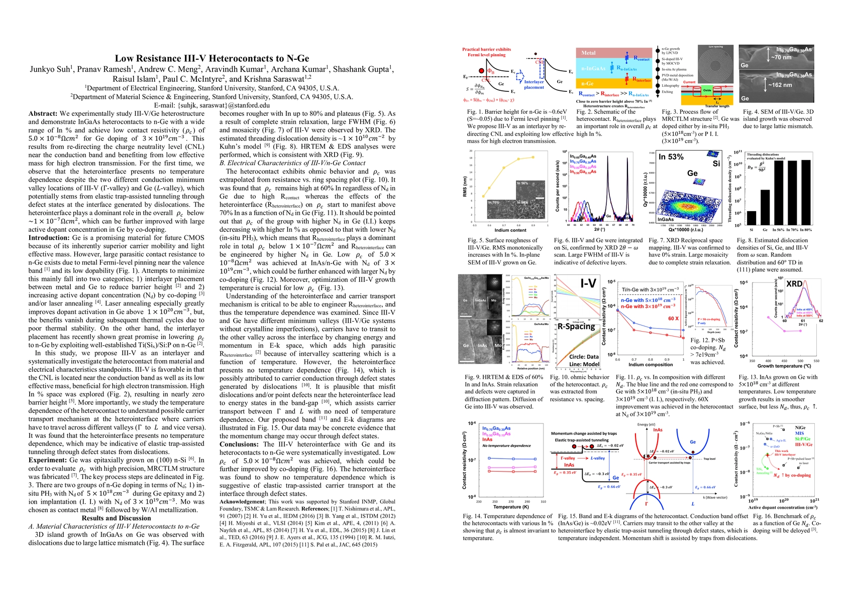
We experimentally study III-V/Ge heterostructure and demonstrate InGaAs hetero-contacts to n-Ge with a wide range of In % and achieve low contact resistivity ($\rho_C$) of $5\times10^{-8} \Omega\cdo...
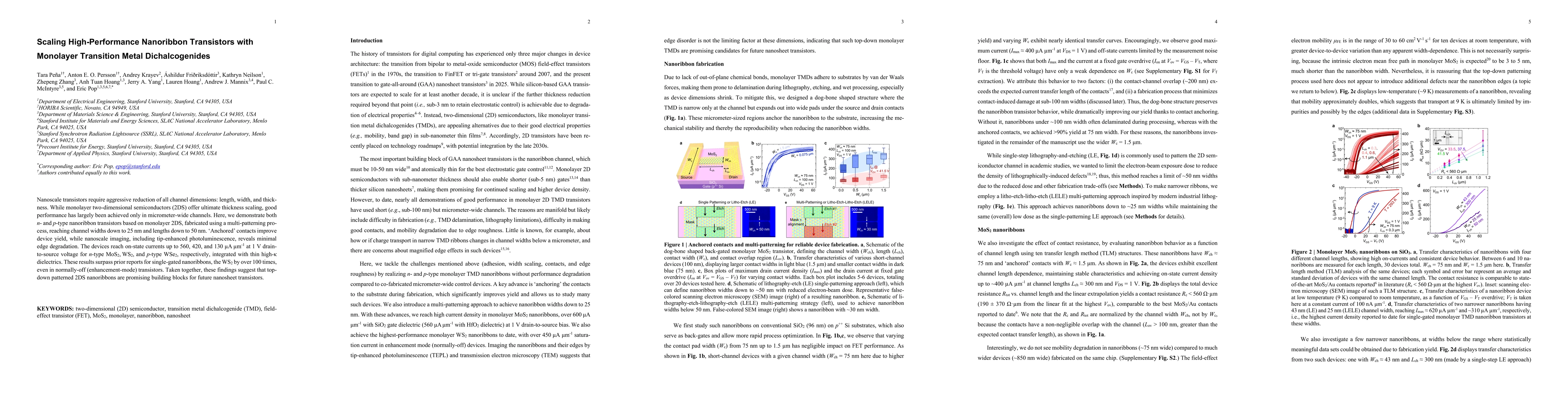
Nanoscale transistors require aggressive reduction of all channel dimensions: length, width, and thickness. While monolayer two-dimensional semiconductors (2DS) offer ultimate thickness scaling, good ...
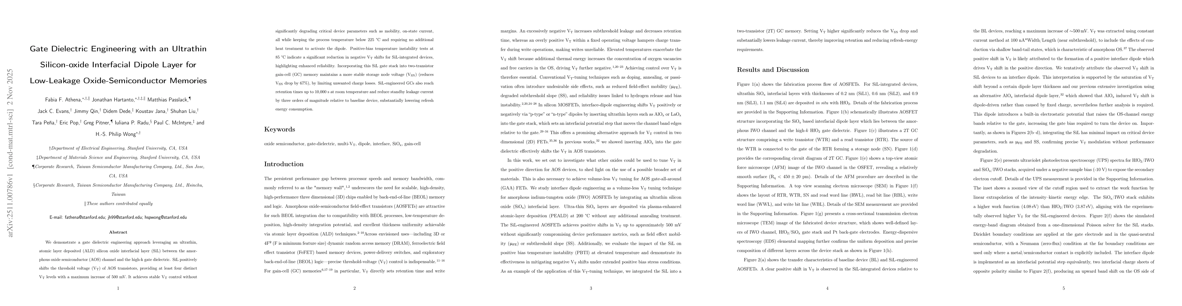
We demonstrate a gate dielectric engineering approach leveraging an ultrathin, atomic layer deposited (ALD) silicon oxide interfacial layer (SiL) between the amorphous oxide semiconductor (AOS) channe...
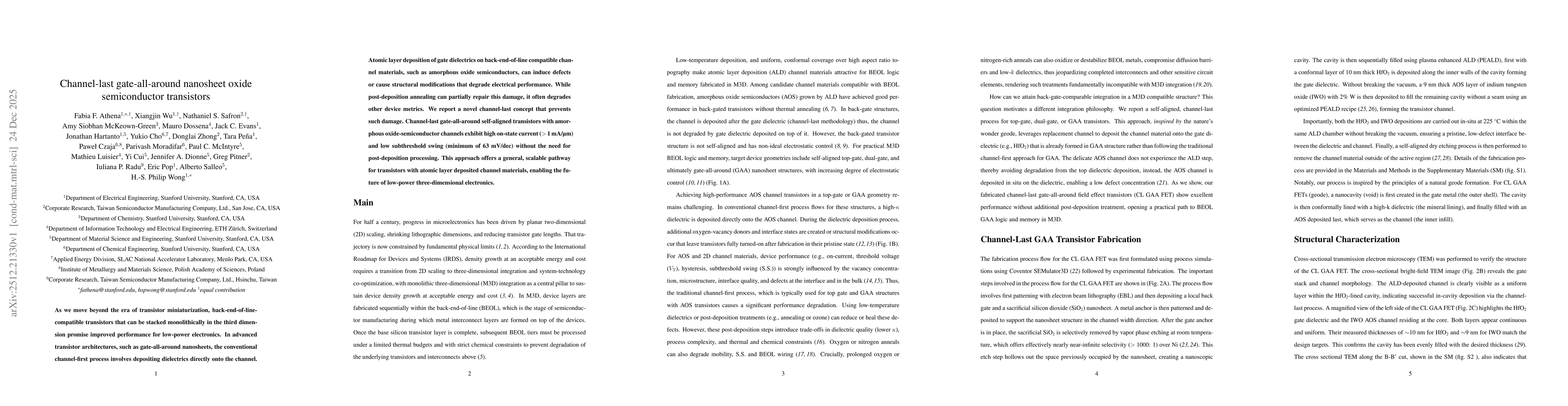
As we move beyond the era of transistor miniaturization, back-end-of-line-compatible transistors that can be stacked monolithically in the third dimension promise improved performance for low-power el...
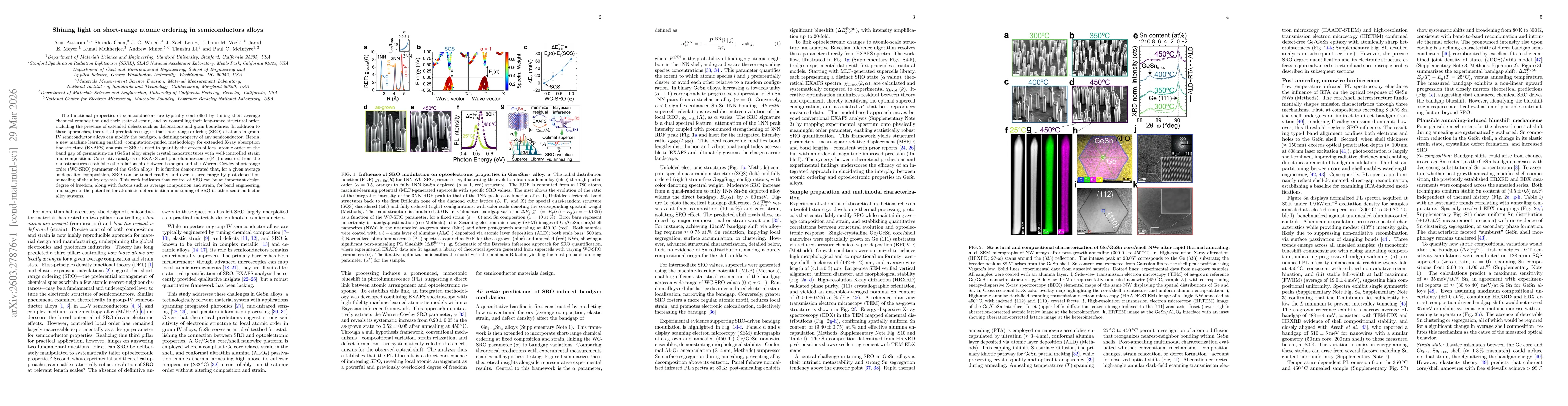
The functional properties of semiconductors are typically controlled by tuning their average chemical composition and their state of strain, and by controlling their long-range structural order, inclu...