Control of faceting during epitaxy is critical for nanoscale devices. This
work identifies the origins of gaps and different facets during regrowth of
InGaAs adjacent to patterned features. Molecular beam epitaxy (MBE) near SiO2
or SiNx led to gaps, roughness, or polycrystalline growth, but metal modulated
epitaxy (MME) produced smooth and gap-free "rising tide" (001) growth filling
up to the mask. The resulting self-aligned FETs were dominated by FET channel
resistance rather than source-drain access resistance. Higher As fluxes led
first to conformal growth, then pronounced {111} facets sloping up away from
the mask.
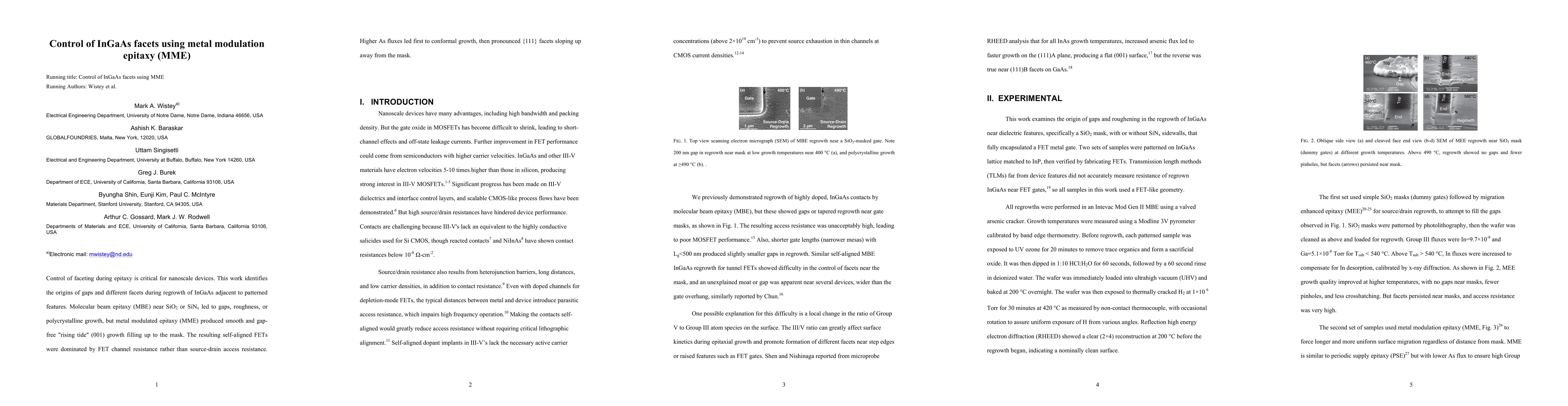
Discussion 0