Academic Profile
Statistics
Similar Authors
Papers on arXiv
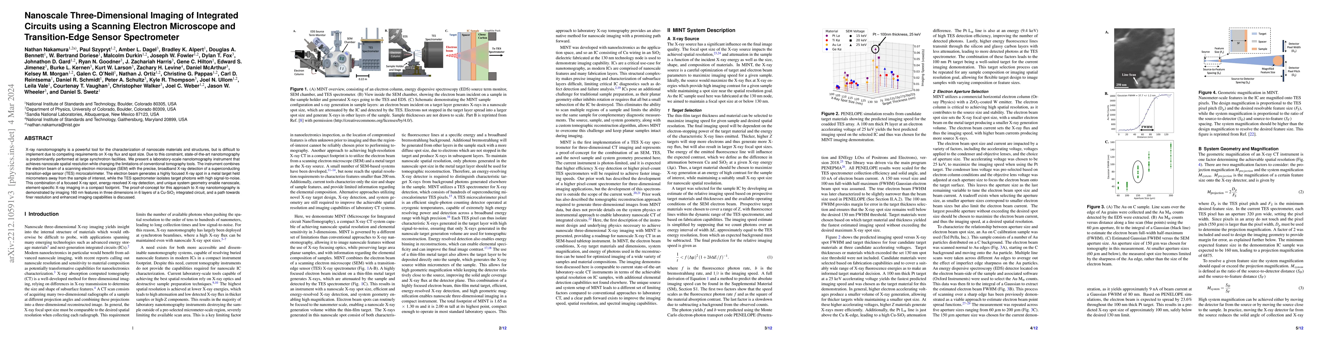
X-ray nanotomography is a powerful tool for the characterization of nanoscale materials and structures, but is difficult to implement due to competing requirements on X-ray flux and spot size. Due t...
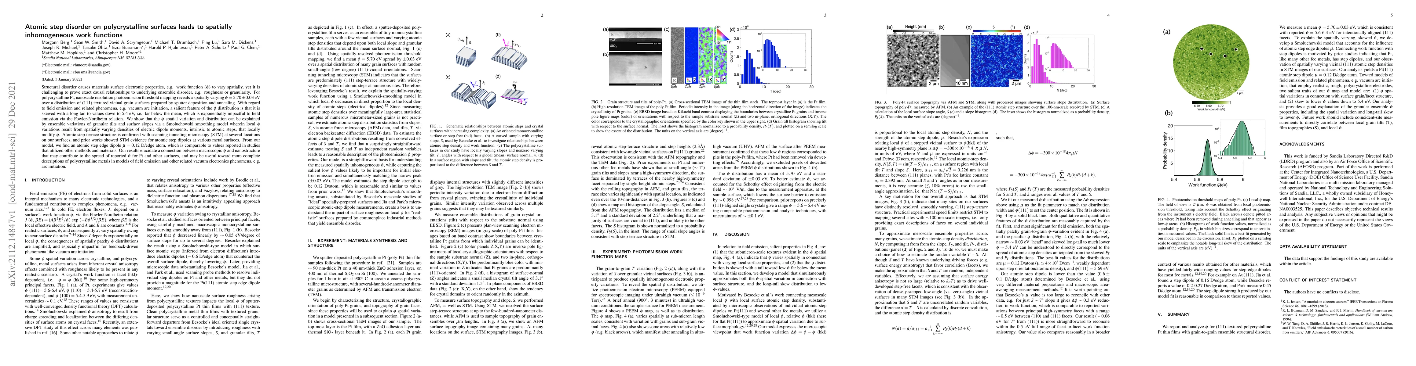
Structural disorder causes materials surface electronic properties, e.g. work function ($\phi$) to vary spatially, yet it is challenging to prove exact causal relationships to underlying ensemble di...
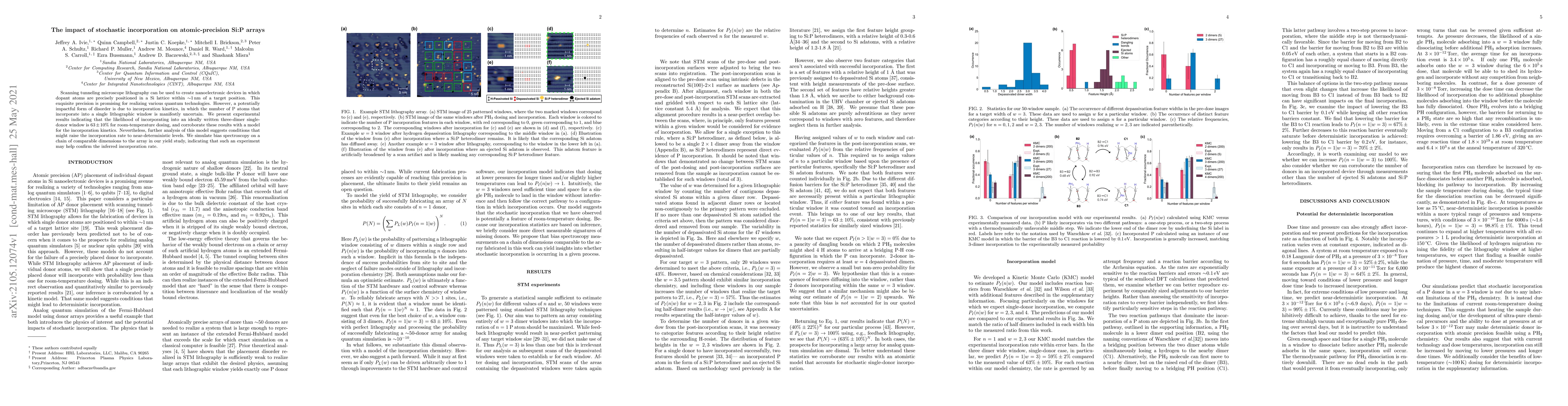
Scanning tunneling microscope lithography can be used to create nanoelectronic devices in which dopant atoms are precisely positioned in a Si lattice within $\sim$1 nm of a target position. This exq...
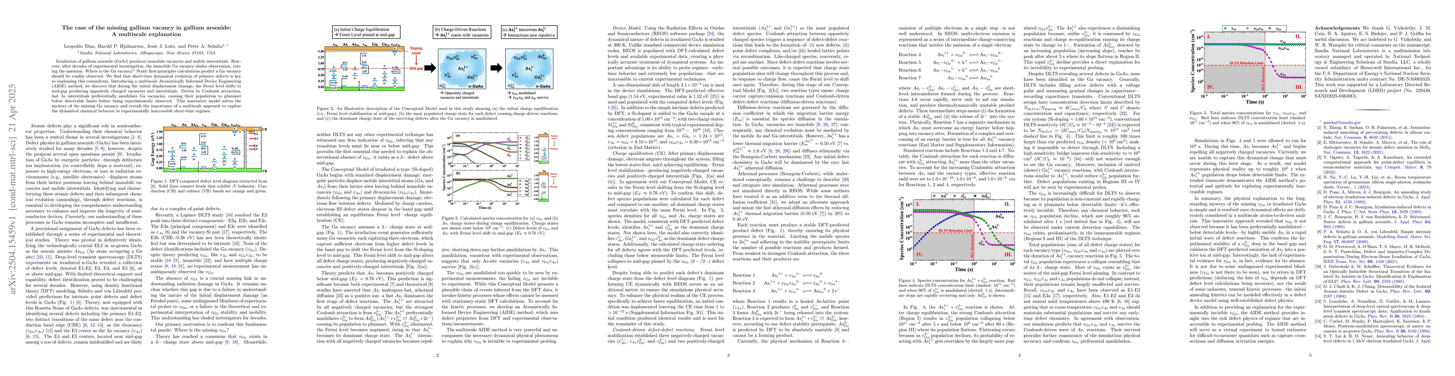
Irradiation of gallium arsenide (GaAs) produces immobile vacancies and mobile interstitials. However, after decades of experimental investigation, the immobile Ga vacancy eludes observation, raising t...
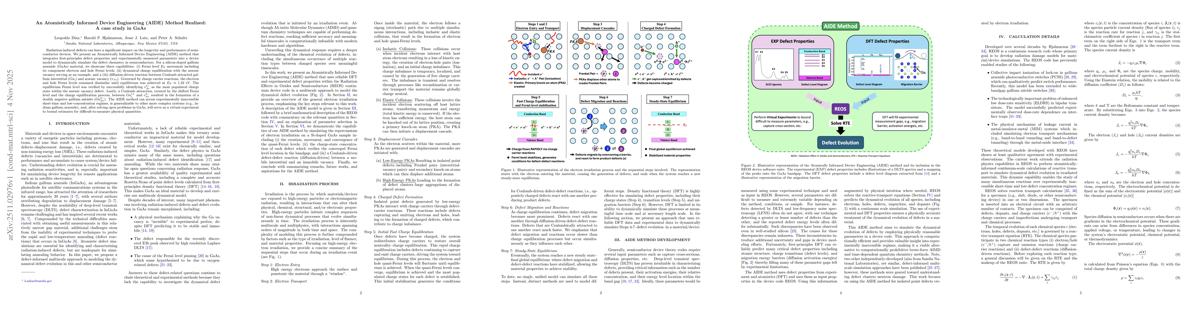
Radiation-induced defects can have a significant impact on the longevity and performance of semiconductor devices. We present an Atomistically Informed Device Engineering (AIDE) method that integrates...