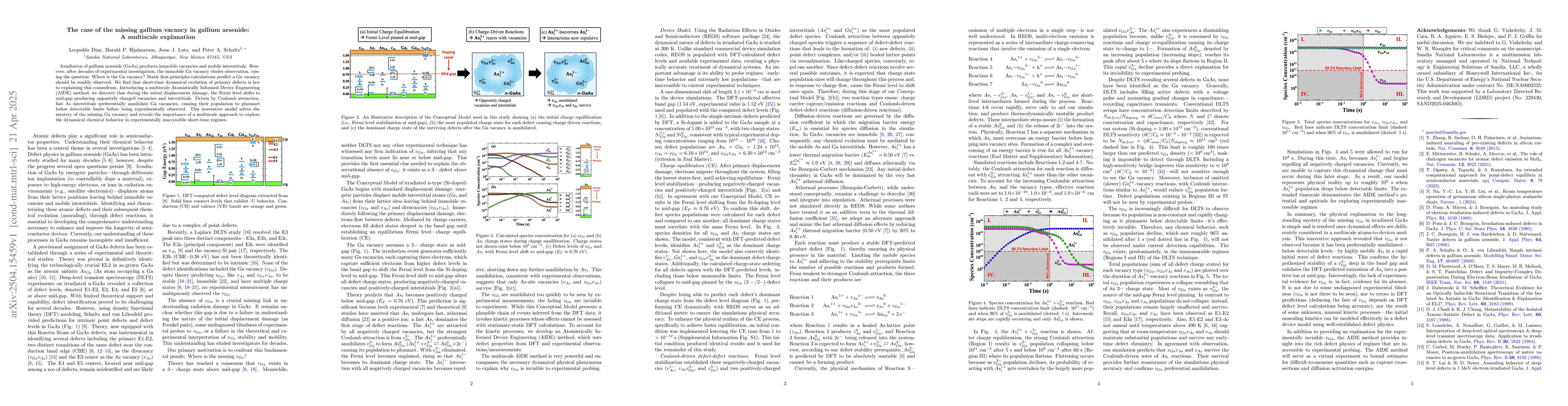
Room temperature operation of germanium-silicon single-photon avalanche diode.
|
Neil Na, Yen-Cheng Lu, Yu-Hsuan Liu, Po-Wei Chen, Ying-Chen Lai, You-Ru Lin, Chung-Chih Lin, T. Shia, Chih-Hao Cheng, Shu-Lu Chen
|
2024
|
View Paper
|
An extended computational approach for point-defect equilibria in semiconductor materials
|
T. Ogawa, Ayako Taguchi, A. Kuwabara
|
2022
|
View Paper
|
Defect and Impurity-Complex Depassivation During Electron-Beam Irradiation of GaAs
|
D. Fleetwood, A. O’Hara, T. Mayer, M. Melloch, S. Pantelides
|
2021
|
View Paper
|
The role of chalcogen vacancies for atomic defect emission in MoS2
|
E. Mitterreiter, B. Schuler, A. Micevic, D. Hernangómez-Pérez, K. Barthelmi, K. Cochrane, J. Kiemle, F. Sigger, J. Klein, E. Wong, E. Barnard, Kenji Watanabe, T. Taniguchi, M. Lorke, F. Jahnke, J. J. Finley, A. Schwartzberg, D. Qiu, S. Refaely-Abramson, A. Holleitner, A. Weber-Bargioni, C. Kastl
|
2020
|
View Paper
|
Laplace DLTS study of the fine structure and metastability of the radiation-induced E3 defect level in GaAs
|
F. Taghizadeh, K. Ostvar, F. D. Auret, W. Meyer
|
2018
|
View Paper
|
Ionization-induced annealing of pre-existing defects in silicon carbide
|
Yanwen Zhang, R. Sachan, O. Pakarinen, M. Chisholm, Peng Liu, H. Xue, W. J. Weber
|
2015
|
View Paper
|
The E1–E2 center in gallium arsenide is the divacancy
|
P. Schultz
|
2015
|
View Paper
|
Model for transport and reaction of defects and carriers within displacement cascades in gallium arsenide
|
W. Wampler, S. Myers
|
2015
|
View Paper
|
Gallium interstitial contributions to diffusion in gallium arsenide
|
J. T. Schick, C. Morgan, P. Papoulias
|
2011
|
View Paper
|
Simple intrinsic defects in gallium arsenide
|
P. Schultz, O. A. von Lilienfeld
|
2009
|
View Paper
|
Ab initio characterization of arsenic vacancy diffusion pathways in GaAs with SIEST-A-RT
|
F. El-Mellouhi, N. Mousseau
|
2007
|
View Paper
|
Charge-dependent migration pathways for the Ga vacancy in GaAs
|
F. El-Mellouhi, N. Mousseau
|
2006
|
View Paper
|
Self-vacancies in gallium arsenide: An ab initio calculation
|
F. El-Mellouhi, N. Mousseau
|
2004
|
View Paper
|
Intrinsic Point Defects, Impurities, and Their Diffusion in Silicon
|
P. Pichler
|
2004
|
View Paper
|
Metastable and nonmetastable recombination-induced defect reactions involving a hydrogen complex with a silicon vacancy in SiC
|
Y. Koshka
|
2004
|
View Paper
|
Mechanisms for radiation dose-rate sensitivity of bipolar transistors
|
H. Hjalmarson, R. Pease, S. C. Witczak, M. Shaneyfelt, J. Schwank, A. Edwards, C. Hembree, T. Mattsson
|
2003
|
View Paper
|
First-principles study of As interstitials in GaAs: Convergence, relaxation, and formation energy
|
J. T. Schick, C. Morgan, P. Papoulias
|
2002
|
View Paper
|
Radiation Effects in Advanced Semiconductor Materials and Devices
|
C. Claeys, E. Simoen
|
2002
|
View Paper
|
Band parameters for III–V compound semiconductors and their alloys
|
I. Vurgaftman, J. Meyer, L. Ram-Mohan
|
2001
|
View Paper
|
Annealing behavior of deep‐level defects in 1 MeV electron irradiated GaAs
|
S. Lai, B. Nener
|
1994
|
View Paper
|
Dopant and defect energetics: Si in GaAs.
|
J. Northrup, Shengbai Zhang
|
1993
|
View Paper
|
Native defects in gallium arsenide
|
J. Bourgoin, H. Bardeleben, D. Stiévenard
|
1988
|
View Paper
|
Positron-annihilation spectroscopy of native vacancies in as-grown GaAs.
|
Corbel, Stucky, Hautojärvi, Saarinen, Moser
|
1988
|
View Paper
|
Metastability of the isolated arsenic-antisite defect in GaAs.
|
D. Chadi, K. Chang
|
1988
|
View Paper
|
Theoretical evidence for an optically inducible structural transition of the isolated As antisite in GaAs: Identification and explanation of EL2?
|
Jaroslaw Dabrowski, Matthias Scheffler
|
1988
|
View Paper
|
Electronic structure, total energies, and abundances of the elementary point defedts in GaAs.
|
G. Baraff, Michael Schlüter
|
1985
|
View Paper
|
Irradiation-induced defects in GaAs
|
D. Pons, J. Bourgoin
|
1985
|
View Paper
|
Interpretation of deep-level optical spectroscopy and deep-level transient spectroscopy data: Application to irradiation defects in GaAs
|
S. Loualiche, A. Nouailhat, G. Guillot, M. Lannoo
|
1984
|
View Paper
|
Capacitance Transient Spectroscopy of Trace Contamination in Silicon
|
J. Benton, L. Kimerling
|
1982
|
View Paper
|
A high sensitivity bridge for the measurement of deep states in semiconductors
|
S. Misrachi, A. Peaker, B. Hamilton
|
1980
|
View Paper
|
An annealing study of electron irradiation‐induced defects in GaAs
|
D. Pons, A. Mircea, J. Bourgoin
|
1980
|
View Paper
|
A new mechanism for interstistitial migration
|
J.C Bourgoin, J.W Corbett
|
1972
|
View Paper
|
The theory of p-n junctions in semiconductors and p-n junction transistors
|
W. Shockley
|
1949
|
View Paper
|
Gallium self-interstitial relaxation in GaAs: An ab initio characterization
|
|
2007
|
|
Semiconductor Material & Device Characterization
|
|
2005
|
|
Handbook of Electronic Materials , Vol. 5 (Plenum, New York
|
|
1971
|
|
Recombination Mechanisms
|
|
1968
|
|
Theory of the flow of electrons & holes in germanium & other semiconductors
|
|
1950
|
|
¨Uber die W¨armebewegung in festen und fl¨ussi-gen K¨orpern
|
|
1926
|
|
Defect Population Size Criteria. Experimentally re-ported defect concentrations for radiation-induced GaAs
|
|
|
|
The divacancy population must be larger than single vacancies v Ga v As > v Ga = v As because the experimentally reported E1-E2 are larger than E3 [5]
|
|
|
|
Fermi level pinning implies that there are equal (or more) available states for dopant electrons ( e ), i.e., the number of available negatively charged vacancy
|
|
|
|
Theory of the metastable injection-bleached E 3 c center in GaAs
|
|
|
|
Comments (0)