ArxivLens
P
Researcher

Pierre-Edouard Raynal

5 papers on arXiv

5 arXiv Papers
28 Total Publications
Profile

Academic Profile

Name P. Raynal
Total Papers 28
Scholar Profile View on Semantic Scholar
Metrics

Statistics

5 arXiv Papers
28 Total Publications
Publications

Papers on arXiv

Thumbnail for Recent Progresses and Perspectives of UV Laser Annealing Technologies
  for Advanced CMOS Devices
arXiv
Recent Progresses and Perspectives of UV Laser Annealing Technologies for Advanced CMOS Devices

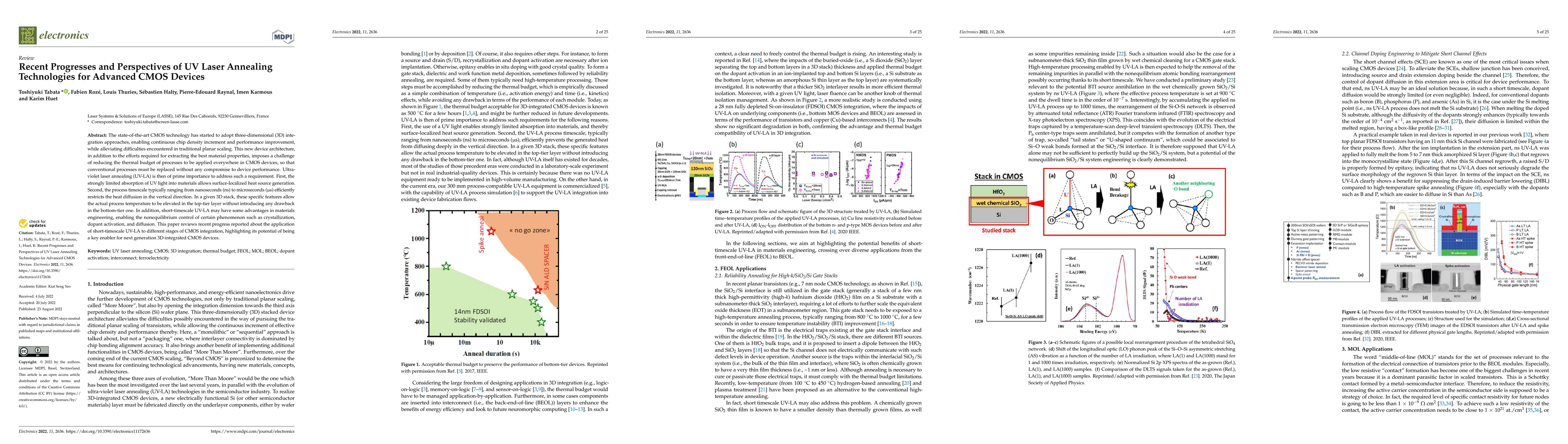
The state-of-the-art CMOS technology has started to adopt three-dimensional (3D) integration approaches, enabling continuous chip density increment and performance improvement, while alleviating dif...

Thumbnail for Microsecond non-melt UV laser annealing for future 3D-stacked CMOS
arXiv
Microsecond non-melt UV laser annealing for future 3D-stacked CMOS

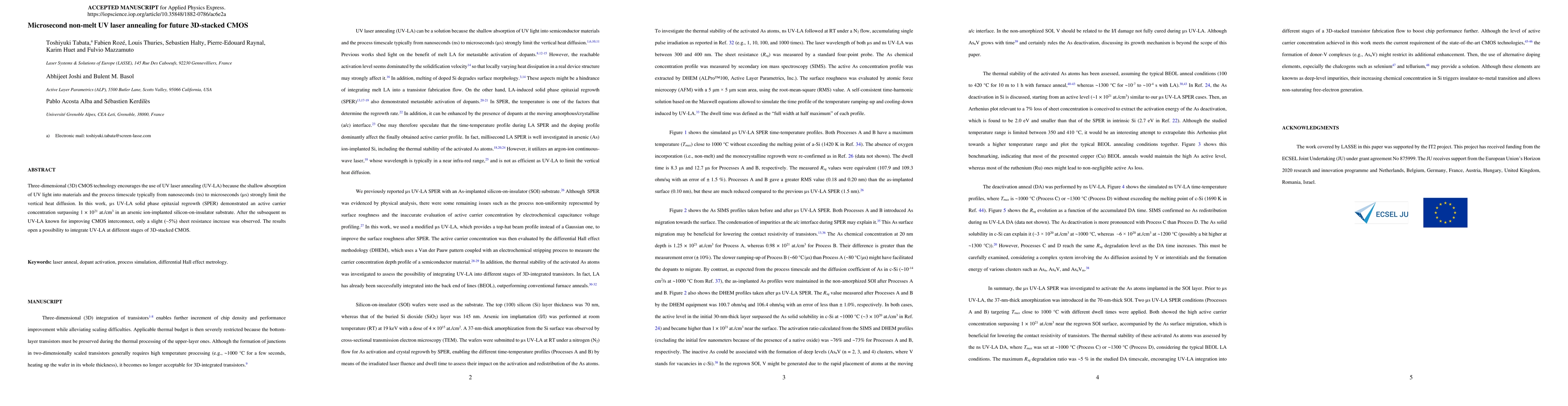
Three-dimensional (3D) CMOS technology encourages the use of UV laser annealing (UV-LA) because the shallow absorption of UV light into materials and the process timescale typically from nanoseconds...

Thumbnail for Solid Phase Recrystallization in Arsenic Ion-Implanted
  Silicon-On-Insulator by Microsecond UV Laser Annealing
arXiv
Solid Phase Recrystallization in Arsenic Ion-Implanted Silicon-On-Insulator by Microsecond UV Laser Annealing

UV laser annealing (UV-LA) enables surface-localized high-temperature thermal processing to form abrupt junctions in emerging monolithically stacked devices, where the applicable thermal budget is r...

Thumbnail for Copper Large-scale Grain Growth by UV Nanosecond Pulsed Laser Annealing
arXiv
Copper Large-scale Grain Growth by UV Nanosecond Pulsed Laser Annealing

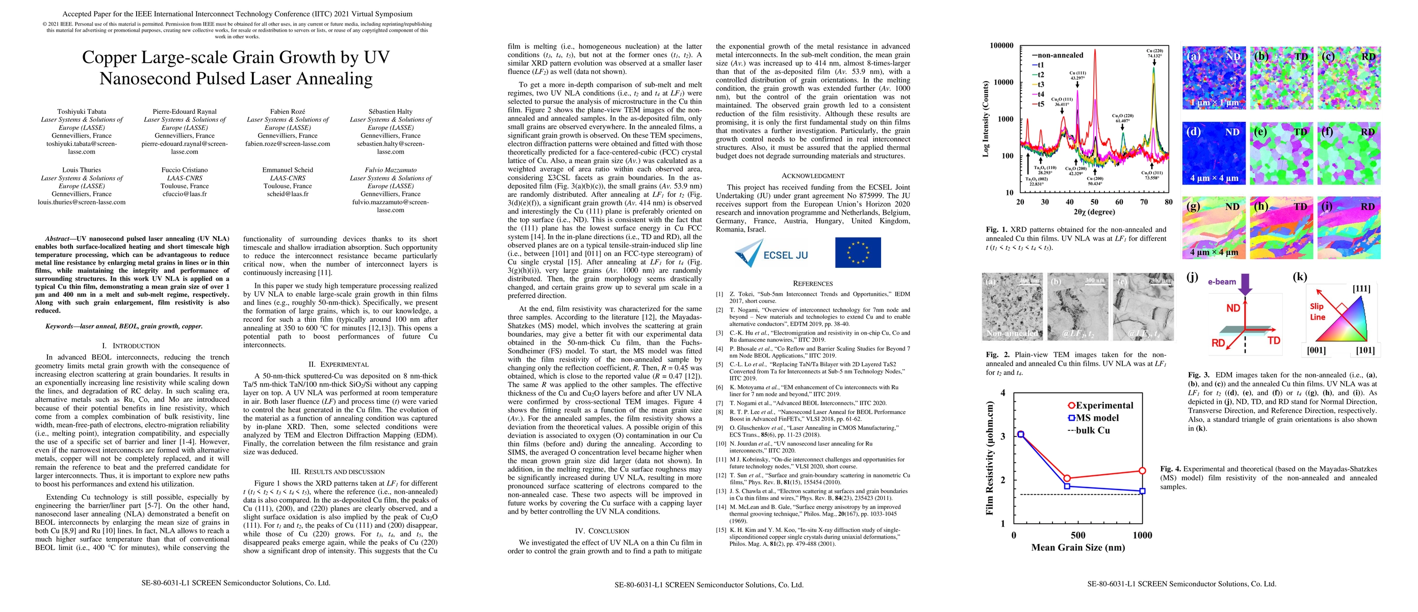
UV nanosecond pulsed laser annealing (UV NLA) enables both surface-localized heating and short timescale high temperature processing, which can be advantageous to reduce metal line resistance by enl...

Thumbnail for Solid Phase Recrystallization and Dopant Activation in Arsenic
  Ion-Implanted Silicon-On-Insulator by UV Laser Annealing
arXiv
Solid Phase Recrystallization and Dopant Activation in Arsenic Ion-Implanted Silicon-On-Insulator by UV Laser Annealing

UV laser annealing (UV-LA) enables surface-localized high-temperature thermal processing to form abrupt junctions in emerging monolithically stacked devices, where applicable thermal budget is restr...

This website uses cookies to ensure you get the best experience. Learn more