Summary
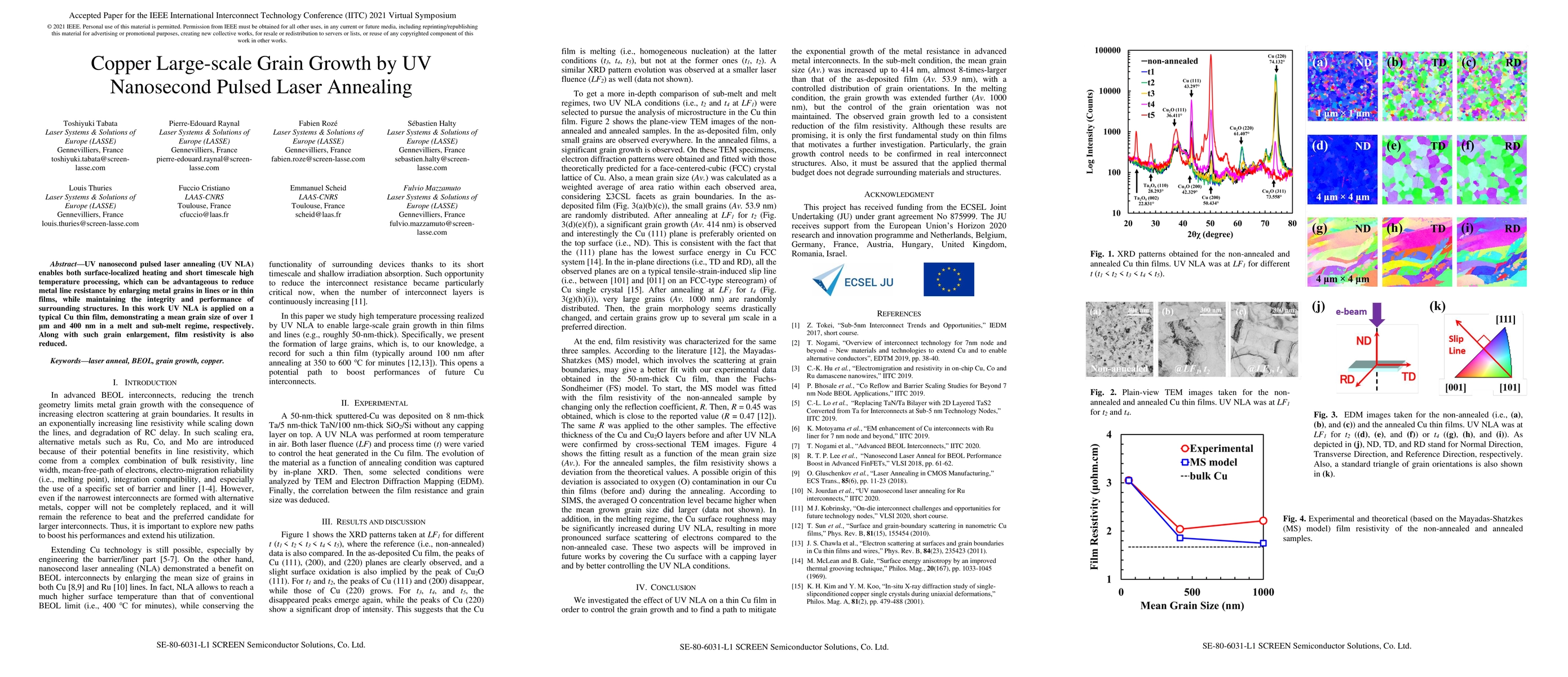
UV nanosecond pulsed laser annealing (UV NLA) enables both surface-localized heating and short timescale high temperature processing, which can be advantageous to reduce metal line resistance by enlarging metal grains in lines or in thin films, while maintaining the integrity and performance of surrounding structures. In this work UV NLA is applied on a typical Cu thin film, demonstrating a mean grain size of over 1 {\mu}m and 400 nm in a melt and sub-melt regime, respectively. Along with such grain enlargement, film resistivity is also reduced.
AI Key Findings - Failed
Key findings generation failed. Failed to start generation process
Paper Details
PDF Preview
Key Terms
Citation Network
Current paper (gray), citations (green), references (blue)
Display is limited for performance on very large graphs.
Similar Papers
Found 4 papersDopant redistribution and activation in Ga ion-implanted high Ge content SiGe by explosive crystallization during UV nanosecond pulsed laser annealing
Karim, Toshiyuki Tabata, Fulvio Mazzamuto et al.
Fractal Carbon nanofoams by nanosecond and femtosecond pulsed-laser deposition
Davide Orecchia, Alessandro Maffini, Margherita Zavelani-Rossi et al.
Nanosecond Laser Annealing: impact on superconducting Silicon on Insulator epilayers
Y. Baron, J. L. Lábár, S. Lequien et al.
| Title | Authors | Year | Actions |
|---|

Comments (0)