Academic Profile
Statistics
Similar Authors
Papers on arXiv
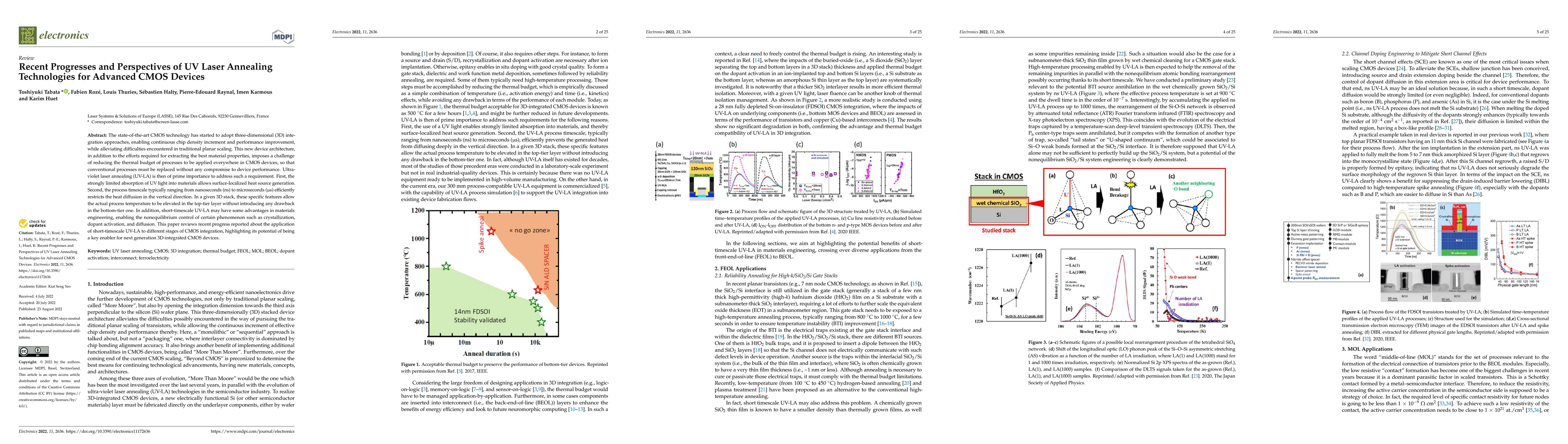
The state-of-the-art CMOS technology has started to adopt three-dimensional (3D) integration approaches, enabling continuous chip density increment and performance improvement, while alleviating dif...
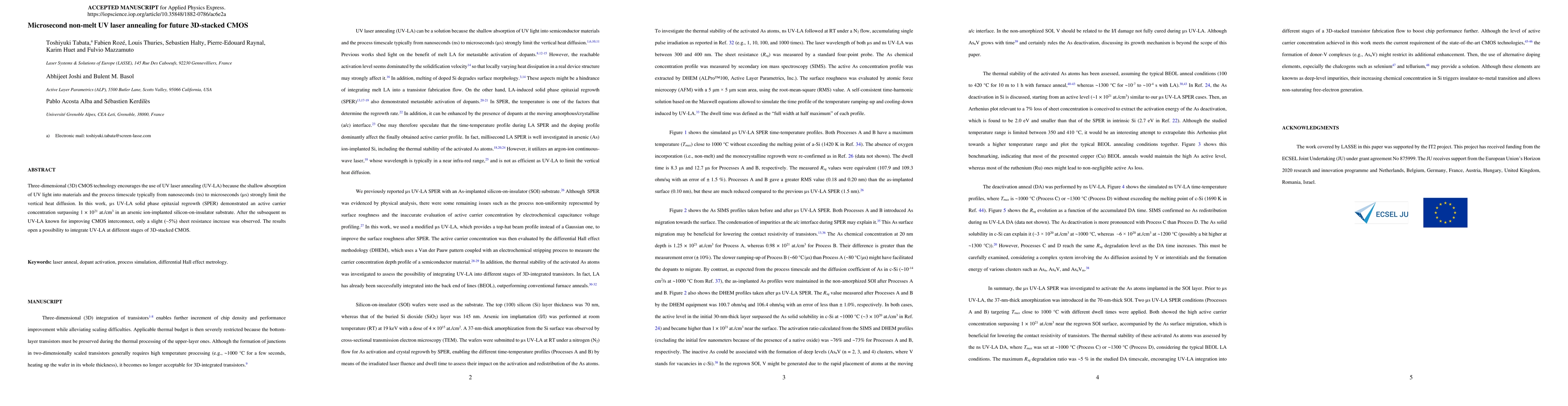
Three-dimensional (3D) CMOS technology encourages the use of UV laser annealing (UV-LA) because the shallow absorption of UV light into materials and the process timescale typically from nanoseconds...
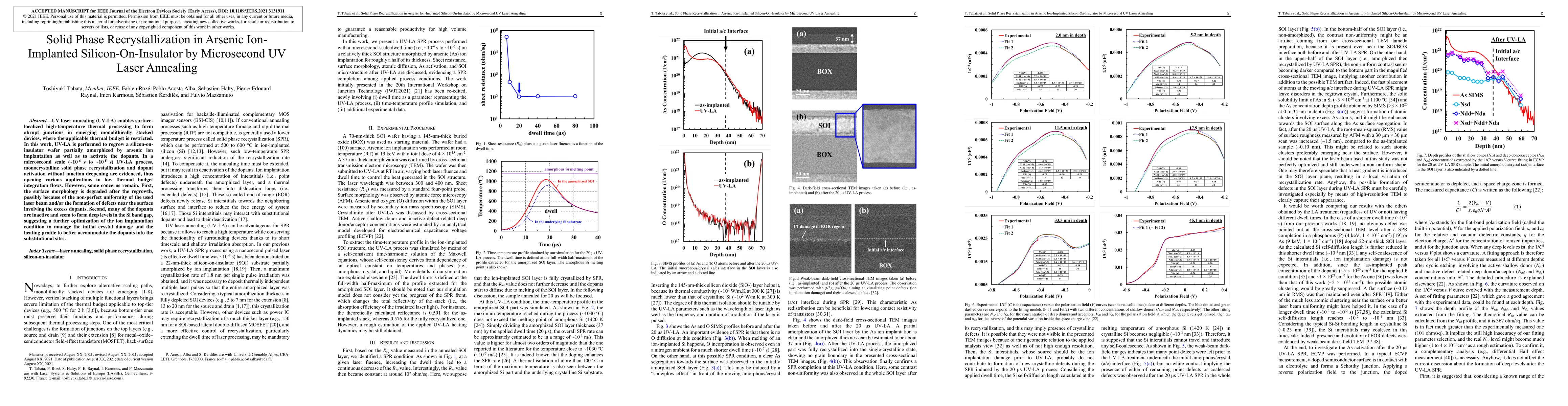
UV laser annealing (UV-LA) enables surface-localized high-temperature thermal processing to form abrupt junctions in emerging monolithically stacked devices, where the applicable thermal budget is r...
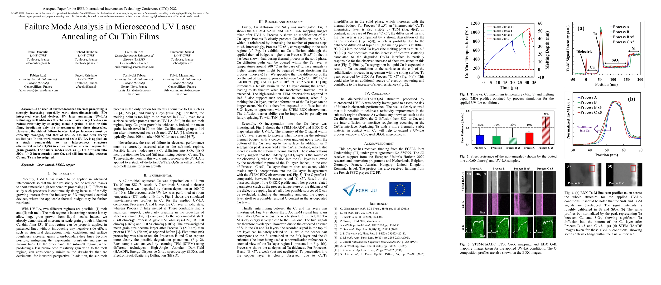
The need of surface-localized thermal processing is strongly increasing especially w.r.t three-dimensionally (3D) integrated electrical devices. UV laser annealing (UV-LA) technology well addresses ...
UV nanosecond pulsed laser annealing (UV NLA) enables both surface-localized heating and short timescale high temperature processing, which can be advantageous to reduce metal line resistance by enl...
UV laser annealing (UV-LA) enables surface-localized high-temperature thermal processing to form abrupt junctions in emerging monolithically stacked devices, where applicable thermal budget is restr...
Explosive crystallization (EC) is often observed when using nanosecond-pulsed melt laser annealing (MLA) in amorphous silicon (Si) and germanium (Ge). The solidification velocity in EC is so fast th...