Failure Mode Analysis in Microsecond UV Laser Annealing of Cu Thin Films
Publication
Metrics
AI Quick Summary
This paper investigates failure modes in microsecond UV laser annealing of Cu thin films used in 3D integrated devices, focusing on Cu diffusion into SiO2, O incorporation into Cu, and intermixing between Cu and Ta to manage electrical performance risks.
Paper Preview
Abstract
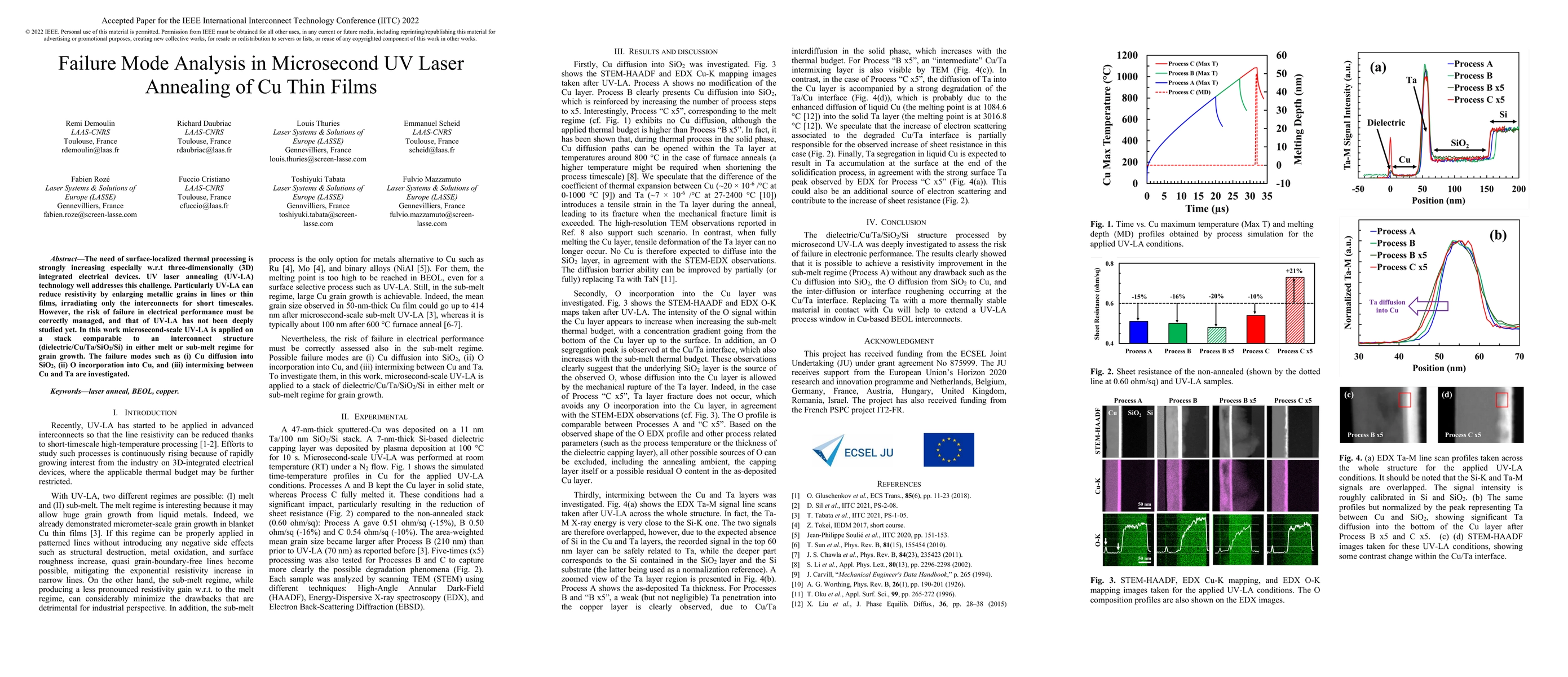
The need of surface-localized thermal processing is strongly increasing especially w.r.t three-dimensionally (3D) integrated electrical devices. UV laser annealing (UV-LA) technology well addresses this challenge. Particularly UV-LA can reduce resistivity by enlarging metallic grains in lines or thin films, irradiating only the interconnects for short timescales. However, the risk of failure in electrical performance must be correctly managed, and that of UV-LA has not been deeply studied yet. In this work microsecond-scale UV-LA is applied on a stack comparable to an interconnect structure (dielectric/Cu/Ta/SiO2/Si) in either melt or sub-melt regime for grain growth. The failure modes such as (i) Cu diffusion into SiO2, (ii) O incorporation into Cu, and (iii) intermixing between Cu and Ta are investigated.
AI Key Findings
Get AI-generated insights about this paper's methodology, results, significance, and more — seven facets brought into focus.
Impact
Paper Details
Authors
PDF Preview
Key Terms
Citation Network
Current paper (gray), citations (green), references (blue)
Display is limited for performance on very large graphs.
Discussion 0