Authors
Summary
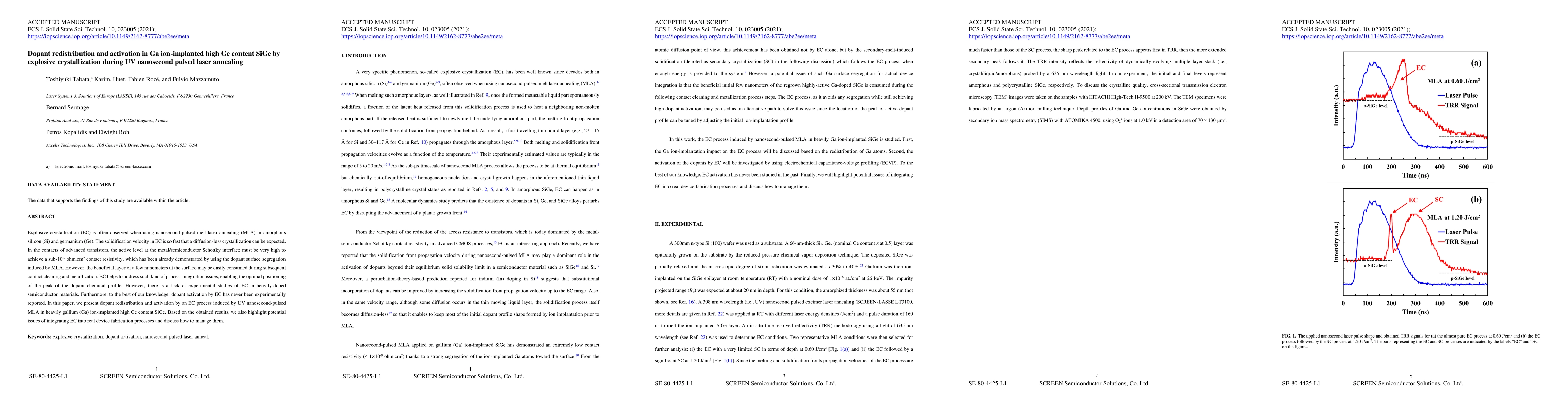
Explosive crystallization (EC) is often observed when using nanosecond-pulsed melt laser annealing (MLA) in amorphous silicon (Si) and germanium (Ge). The solidification velocity in EC is so fast that a diffusion-less crystallization can be expected. In the contacts of advanced transistors, the active level at the metal/semiconductor Schottky interface must be very high to achieve a sub-10^{-9} ohm.cm2 contact resistivity, which has been already demonstrated by using the dopant surface segregation induced by MLA. However, the beneficial layer of a few nanometers at the surface may be easily consumed during subsequent contact cleaning and metallization. EC helps to address such kind of process integration issues, enabling the optimal positioning of the peak of the dopant chemical profile. However, there is a lack of experimental studies of EC in heavily-doped semiconductor materials. Furthermore, to the best of our knowledge, dopant activation by EC has never been experimentally reported. In this paper, we present dopant redistribution and activation by an EC process induced by UV nanosecond-pulsed MLA in heavily gallium (Ga) ion-implanted high Ge content SiGe. Based on the obtained results, we also highlight potential issues of integrating EC into real device fabrication processes and discuss how to manage them.
AI Key Findings
Get AI-generated insights about this paper's methodology, results, and significance.
Paper Details
PDF Preview
Key Terms
Citation Network
Current paper (gray), citations (green), references (blue)
Display is limited for performance on very large graphs.
Similar Papers
Found 4 papersThermal activation of low-density Ga implanted in Ge
Tzu-Ming Lu, Natalie D. Foster, Dwight R. Luhman et al.
Solid Phase Recrystallization in Arsenic Ion-Implanted Silicon-On-Insulator by Microsecond UV Laser Annealing
Toshiyuki Tabata, Fulvio Mazzamuto, Fabien Rozé et al.
| Title | Authors | Year | Actions |
|---|
Comments (0)