Academic Profile
Statistics
Similar Authors
Papers on arXiv
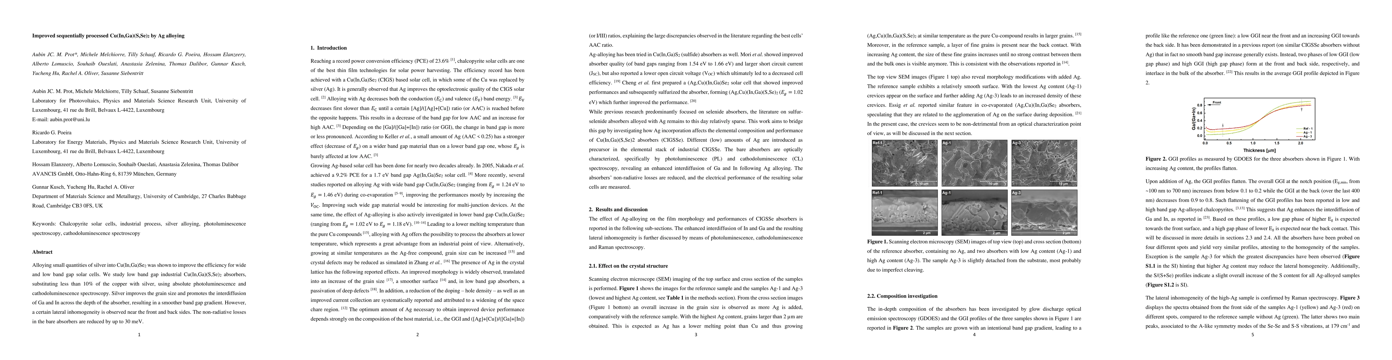
Alloying small quantities of silver into Cu(In,Ga)Se2 was shown to improve the efficiency for wide and low band gap solar cells. We study low band gap industrial Cu(In,Ga)(S,Se)2 absorbers, substitu...
Record efficiency in chalcopyrite-based solar cells Cu(In,Ga)(S,Se)2 is achieved using a gallium gradient to increase the band gap of the absorber towards the back side. Although this structure has ...
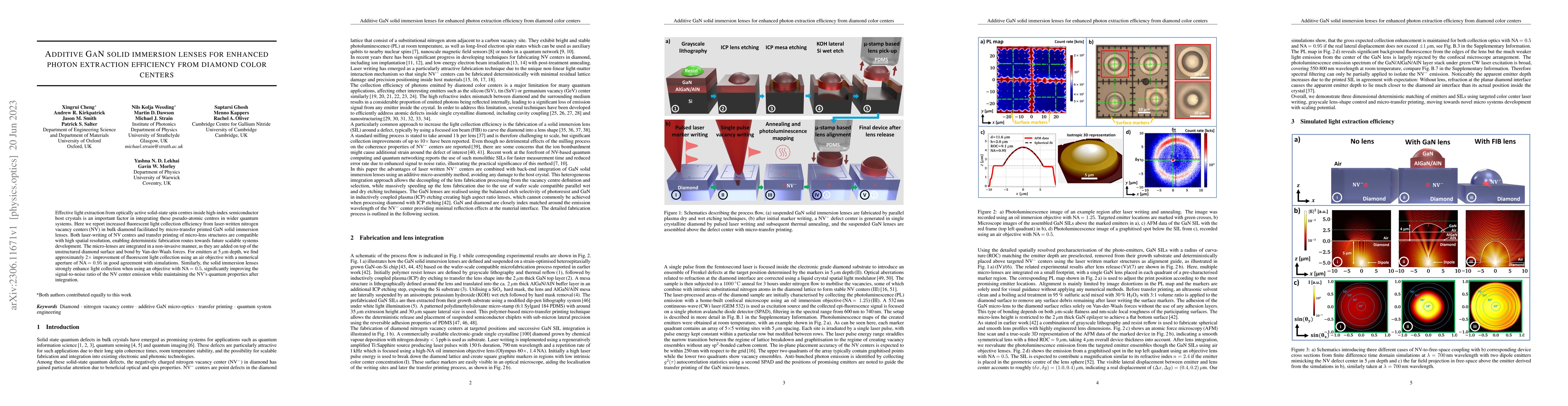
Effective light extraction from optically active solid-state spin centres inside high-index semiconductor host crystals is an important factor in integrating these pseudo-atomic centres in wider qua...
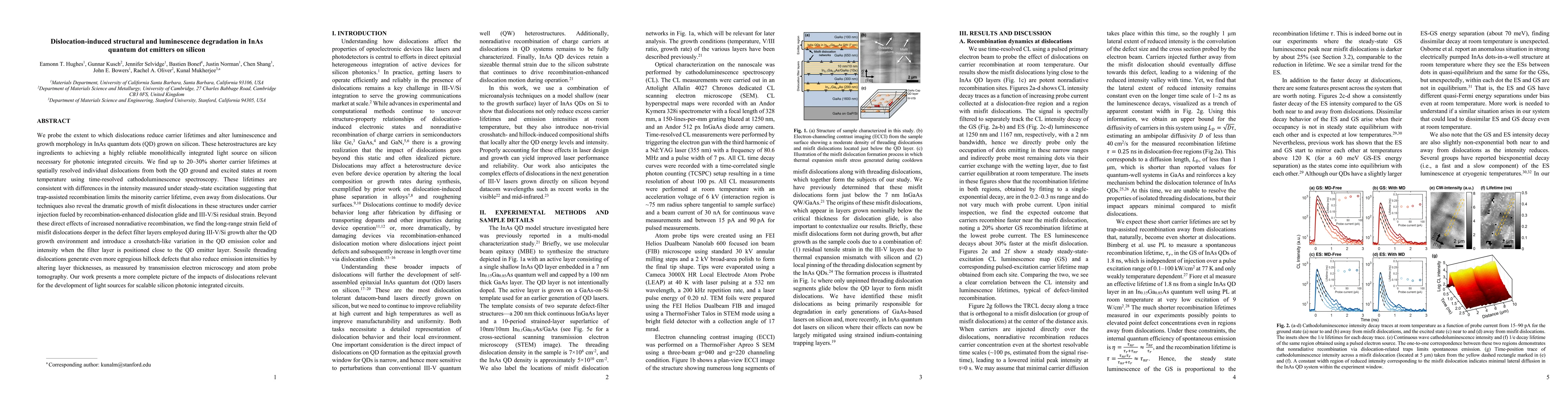
We probe the extent to which dislocations reduce carrier lifetimes and alter luminescence and growth morphology in InAs quantum dots (QD) grown on silicon. These heterostructures are key ingredients...
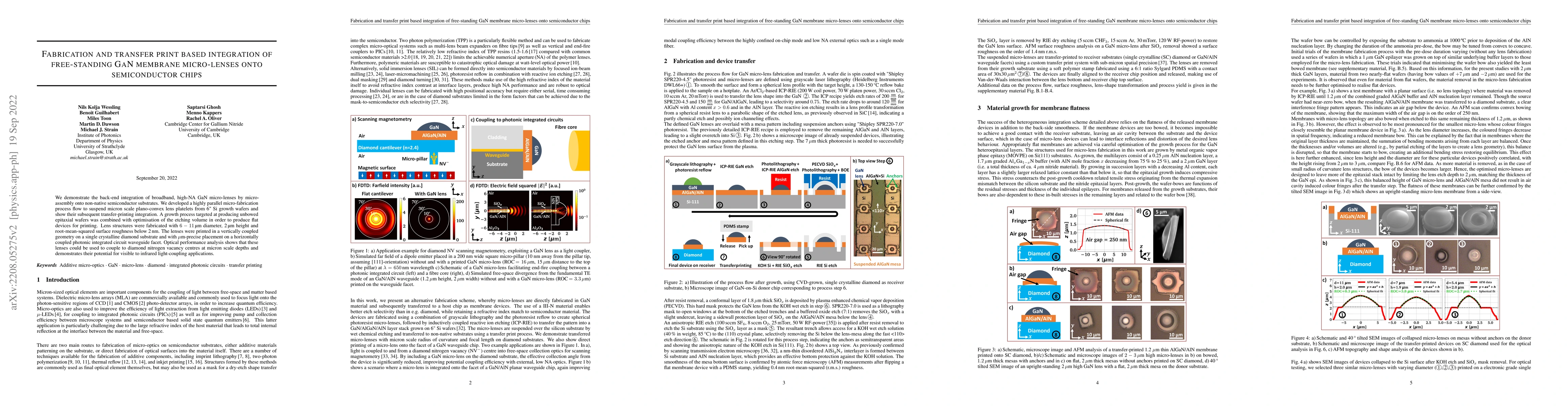
We demonstrate the back-end integration of broadband, high-NA GaN micro-lenses by micro-assembly onto non-native semiconductor substrates. We developed a highly parallel micro-fabrication process fl...
We demonstrate that semiconductor quantum dots can be excited efficiently in a resonant three-photon process, whilst resonant two-photon excitation is highly suppressed. Time-dependent Floquet theor...
Alessandro Strumia recently published a survey of gender differences in publications and citations in high-energy physics (HEP). In addition to providing full access to the data, code, and methodolo...
Diamond heat-spreaders for gallium nitride (GaN) devices currently depend upon a robust wafer bonding process. Bonding-free membrane methods demonstrate potential, however, chemical vapour depositio...
We studied the magnetic properties of ferromagnetic-semiconductor composites based on nickel and porous-GaN, motivated by the effort to couple magnetic and semiconductor functionality. Nickel-infilt...
We present a detailed theoretical analysis of the electronic and optical properties of c-plane InGaN/GaN quantum well structures with In contents ranging from 5% to 25%. Special attention is paid to...
Non-polar (11-20) a-plane quantum dots (QDs) are strong candidates for both > 200 K on-chip ultrafast polarized single-photon generation and the investigation of high temperature semiconductor QD ph...
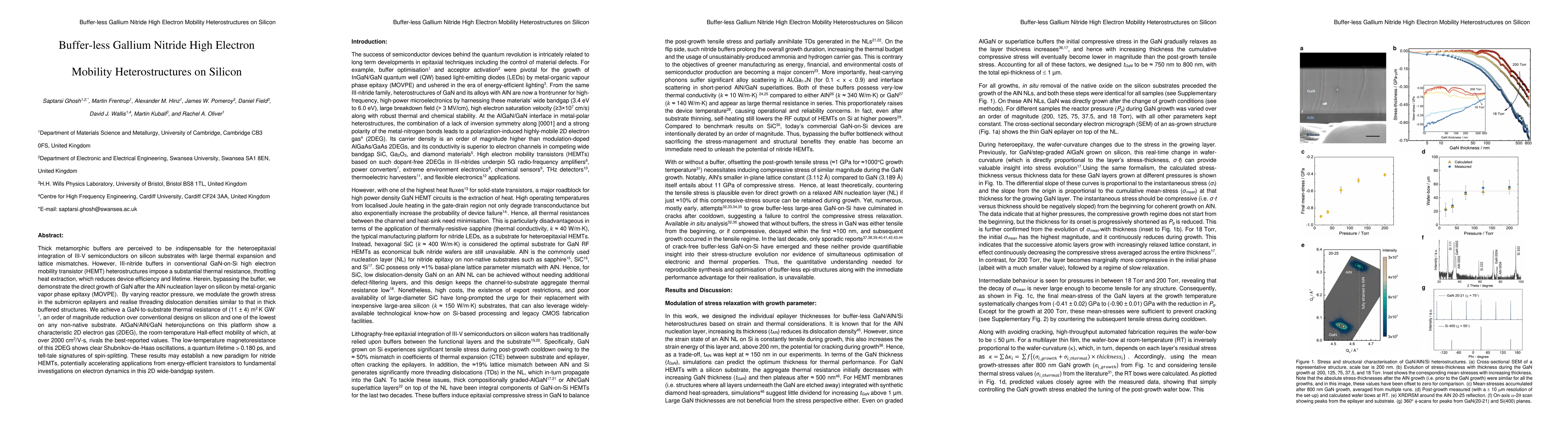
Thick metamorphic buffers are perceived to be indispensable for the heteroepitaxial integration of III-V semiconductors on silicon substrates with large thermal expansion and lattice mismatches. Howev...
The radiative open circuit voltage loss in a solar cell occurs because the absorptance spectrum near the band gap shows gradual increase rather than sharp step function like transition. This broadenin...
This study underscores the pivotal role of sodium (Na) supply in optimizing the optoelectronic properties of wide bandgap (~1.6 eV) Cu(In,Ga)S2 (CIGS) thin film absorbers for high efficiency solar cel...
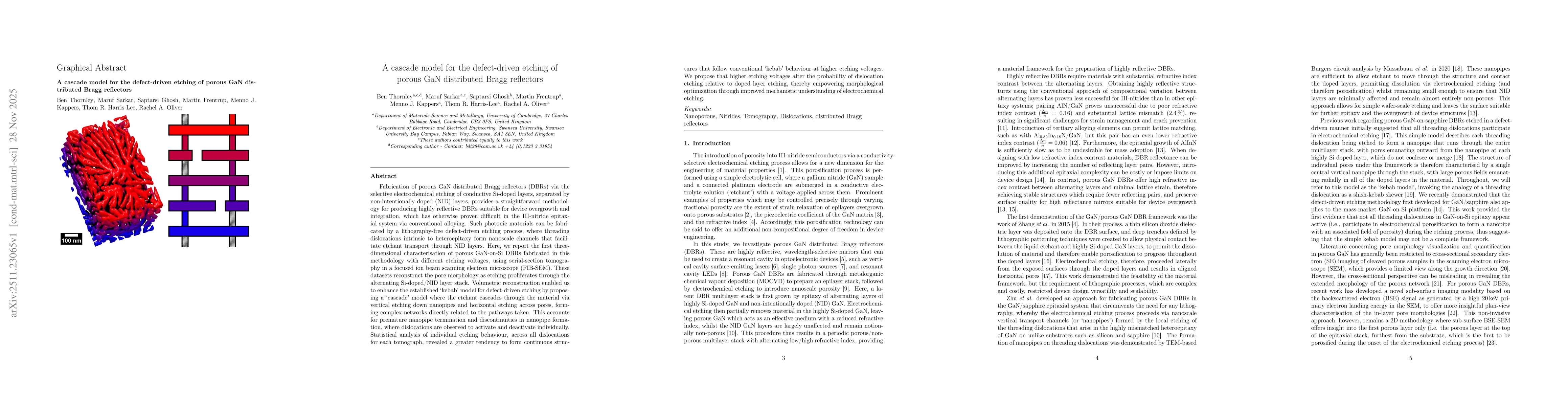
Fabrication of porous GaN distributed Bragg reflectors (DBRs) via the selective electrochemical etching (ECE) of conductive Si-doped layers, separated by non-intentionally doped (NID) layers, provides...
Sulfide chalcopyrite Cu(In,Ga)S2 (CIGS) is a wide bandgap semiconductor suitable for the top cell of a tandem solar device. Here we demonstrate significant improvements in absorber quality by alloying...
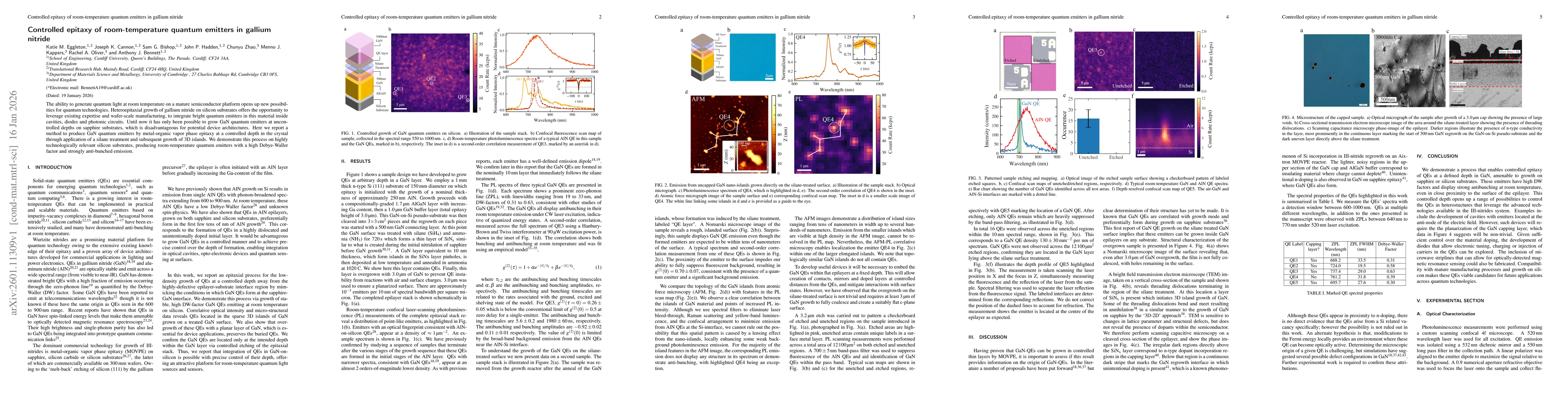
The ability to generate quantum light at room temperature on a mature semiconductor platform opens up new possibilities for quantum technologies. Heteroepitaxial growth of gallium nitride on silicon s...
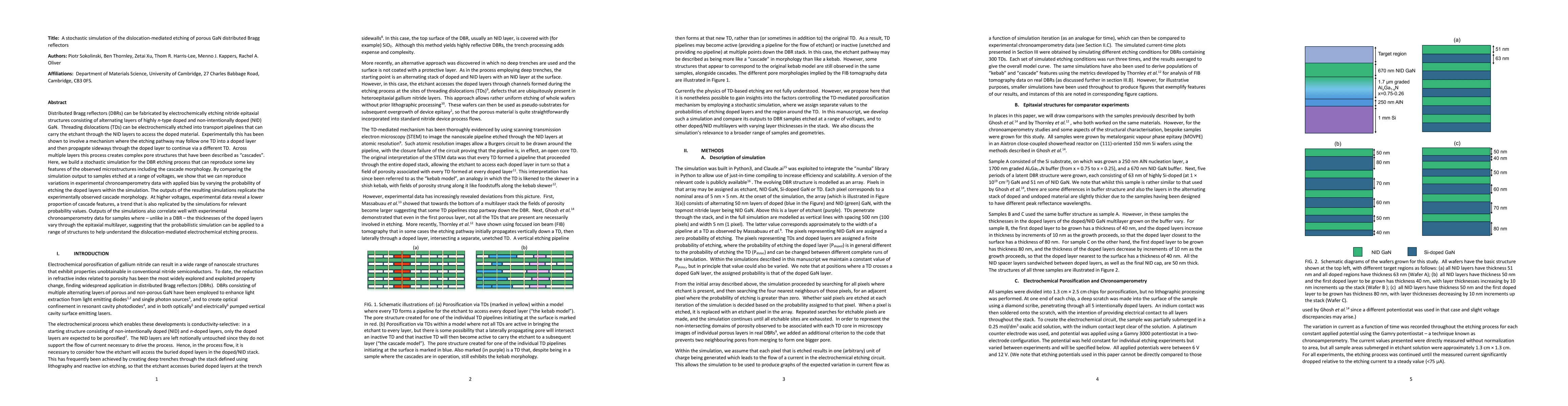
Distributed Bragg reflectors (DBRs) can be fabricated by electrochemically etching nitride epitaxial structures consisting of alternating layers of highly n-type doped and non-intentionally doped (NID...
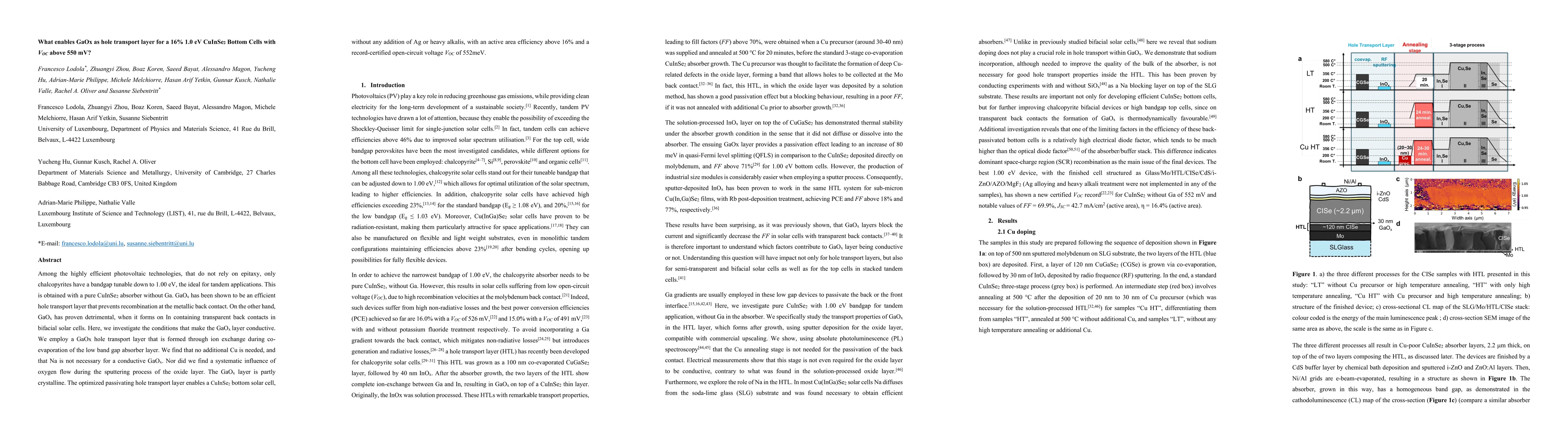
Among the highly efficient photovoltaic technologies, that do not rely on epitaxy, only chalcopyrites have a bandgap tunable down to 1.00 eV, the ideal for tandem applications. This is obtained with a...
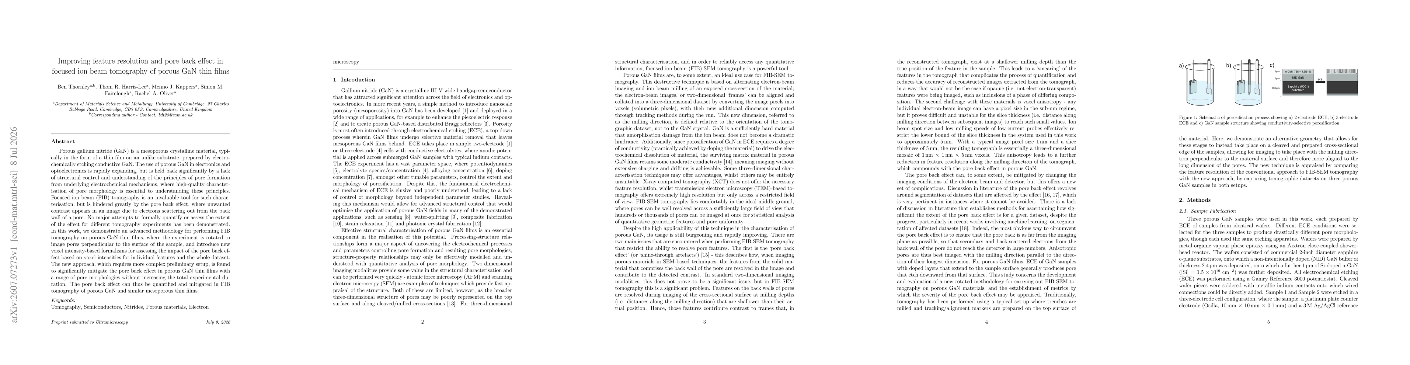
Porous gallium nitride (GaN) is a mesoporous crystalline material, typically in the form of a thin film on an unlike substrate, prepared by electrochemically etching conductive GaN. The use of porous ...