Publication
Metrics
AI Quick Summary
This study investigates how dislocations in InAs quantum dot emitters on silicon degrade carrier lifetimes and luminescence, revealing up to 20-30% shorter lifetimes at dislocations due to trap-assisted recombination. It also highlights how misfit dislocations affect QD growth and emission properties, introducing color and intensity variations, and sessile threading dislocations causing hillock defects that further reduce emission intensities.
Paper Preview
Abstract
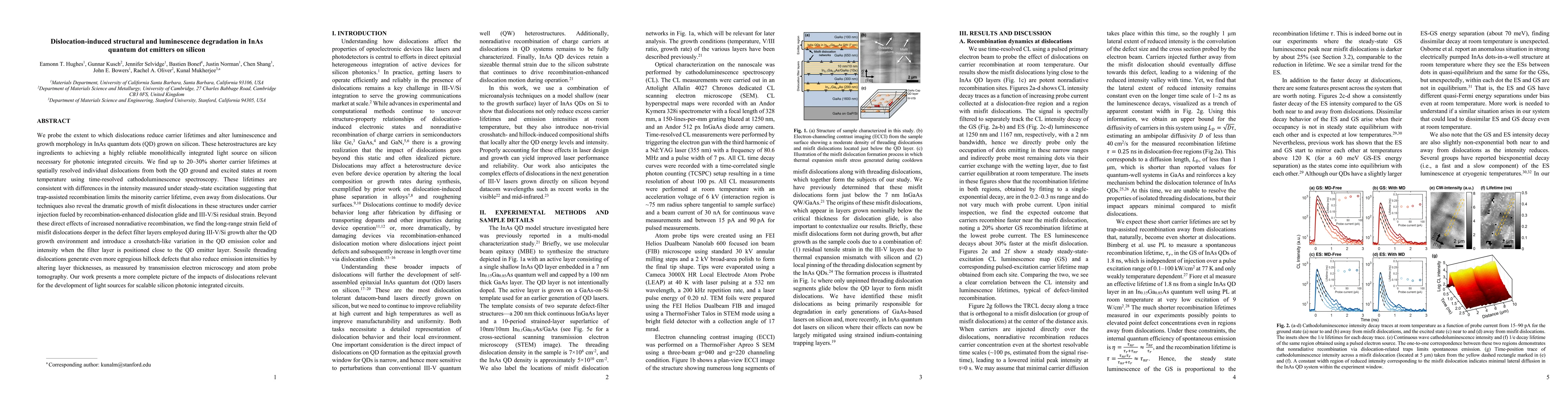
We probe the extent to which dislocations reduce carrier lifetimes and alter luminescence and growth morphology in InAs quantum dots (QD) grown on silicon. These heterostructures are key ingredients to achieving a highly reliable monolithically integrated light source on silicon necessary for photonic integrated circuits. We find up to 20-30% shorter carrier lifetimes at spatially resolved individual dislocations from both the QD ground and excited states at room temperature using time-resolved cathodoluminescence spectroscopy. These lifetimes are consistent with differences in the intensity measured under steady-state excitation suggesting that trap-assisted recombination limits the minority carrier lifetime, even away from dislocations. Our techniques also reveal the dramatic growth of misfit dislocations in these structures under carrier injection fueled by recombination-enhanced dislocation glide and III-V/Si residual strain. Beyond these direct effects of increased nonradiative recombination, we find the long-range strain field of misfit dislocations deeper in the defect filter layers employed during III-V/Si growth alter the QD growth environment and introduce a crosshatch-like variation in the QD emission color and intensity when the filter layer is positioned close to the QD emitter layer. Sessile threading dislocations generate even more egregious hillock defects that also reduce emission intensities by altering layer thicknesses, as measured by transmission electron microscopy and atom probe tomography. Our work presents a more complete picture of the impacts of dislocations relevant for the development of light sources for scalable silicon photonic integrated circuits.
AI Key Findings
Get AI-generated insights about this paper's methodology, results, significance, and more — seven facets brought into focus.
Impact
Paper Details
Authors
PDF Preview
Key Terms
Citation Network
Current paper (gray), citations (green), references (blue)
Display is limited for performance on very large graphs.
Discussion 0