Academic Profile
Statistics
Similar Authors
Papers on arXiv
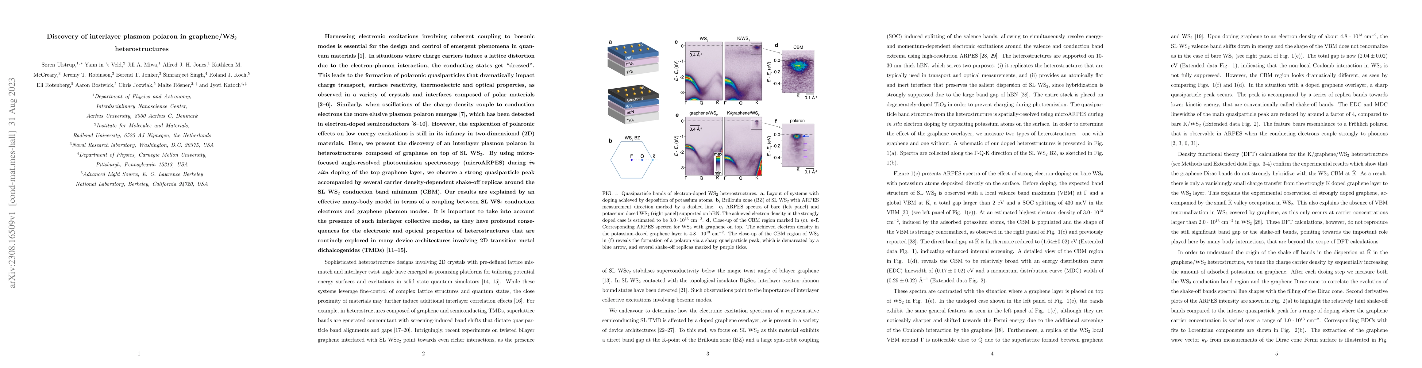
Harnessing electronic excitations involving coherent coupling to bosonic modes is essential for the design and control of emergent phenomena in quantum materials [1]. In situations where charge carr...
Massive Dirac fermions are low-energy electronic excitations characterized by a hyperbolic band dispersion. They play a central role in several emerging physical phenomena such as topological phase ...
A scalable platform to synthesize ultrathin heavy metals may enable high efficiency charge-to-spin conversion for next-generation spintronics. Here we report centimeter-scale synthesis of air-stable...
A mismatch of atomic registries between single-layer transition metal dichalcogenides (TMDs) in a two dimensional van der Waals heterostructure produces a moir\'e superlattice with a periodic potent...
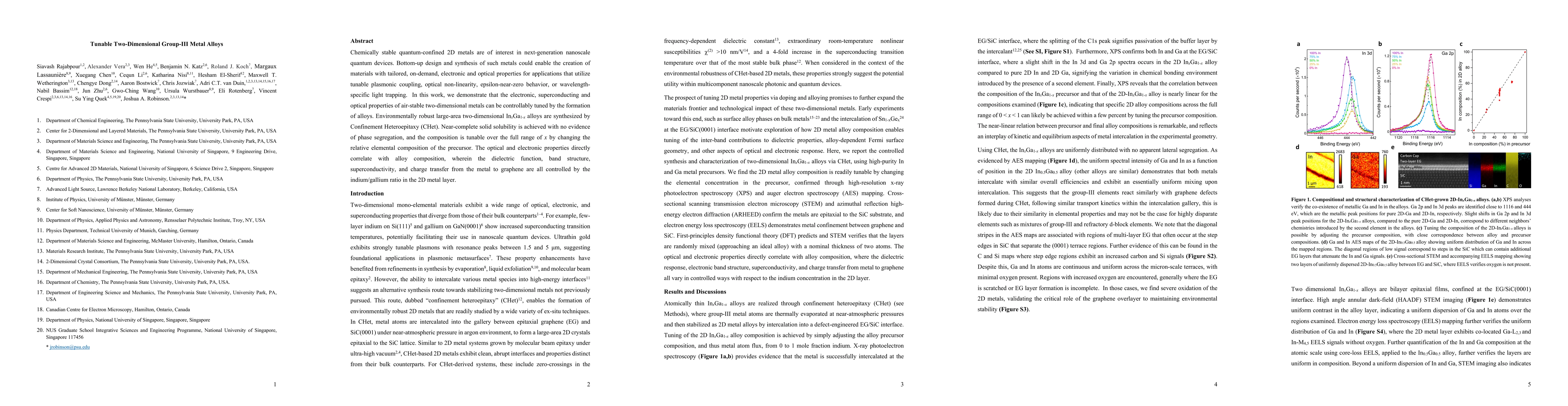
Chemically stable quantum-confined 2D metals are of interest in next-generation nanoscale quantum devices. Bottom-up design and synthesis of such metals could enable the creation of materials with t...
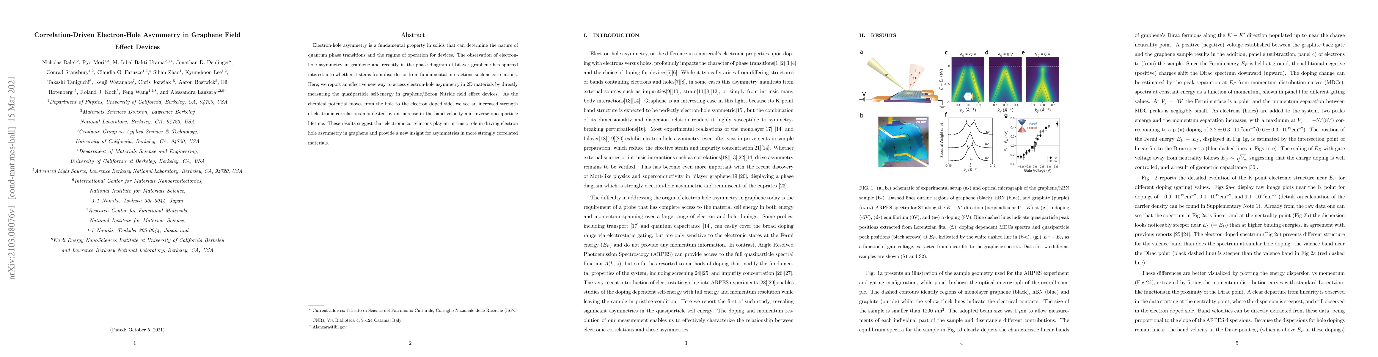
Electron-hole asymmetry is a fundamental property in solids that can determine the nature of quantum phase transitions and the regime of operation for devices. The observation of electron-hole asymm...
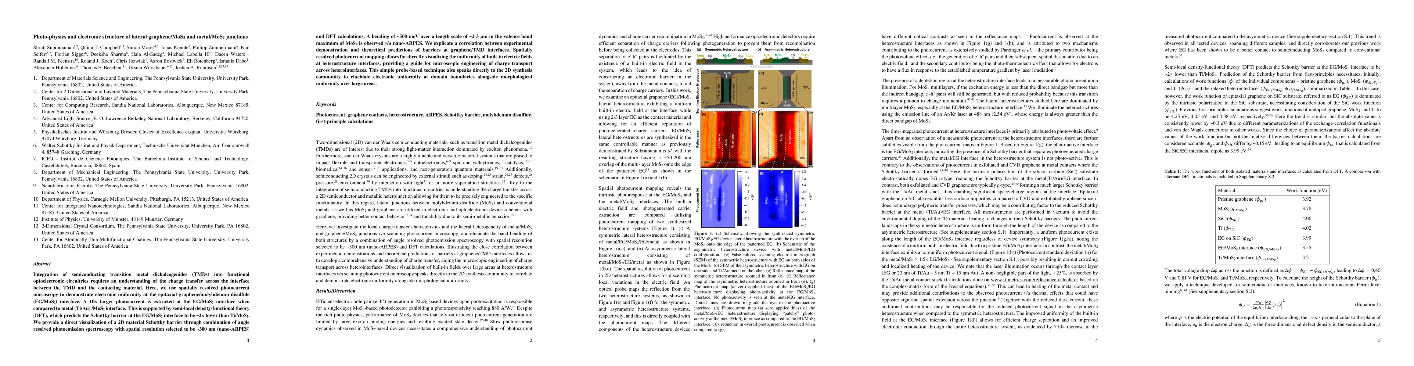
Integration of semiconducting transition metal dichalcogenides (TMDs) into functional optoelectronic circuitries requires an understanding of the charge transfer across the interface between the TMD...
Control of impurity concentrations in semiconducting materials is essential to device technology. Because of their intrinsic confinement, the properties of two-dimensional semiconductors such as tra...
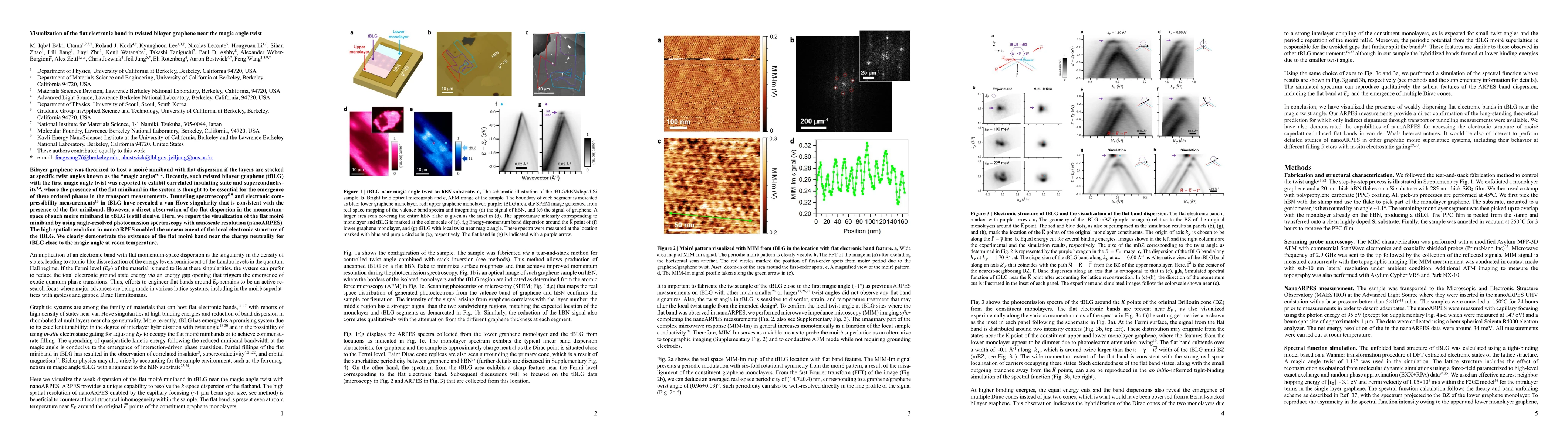
Bilayer graphene was theorized to host a moire miniband with flat dispersion if the layers are stacked at specific twist angles known as the magic angles. Recently, such twisted bilayer graphene (tB...
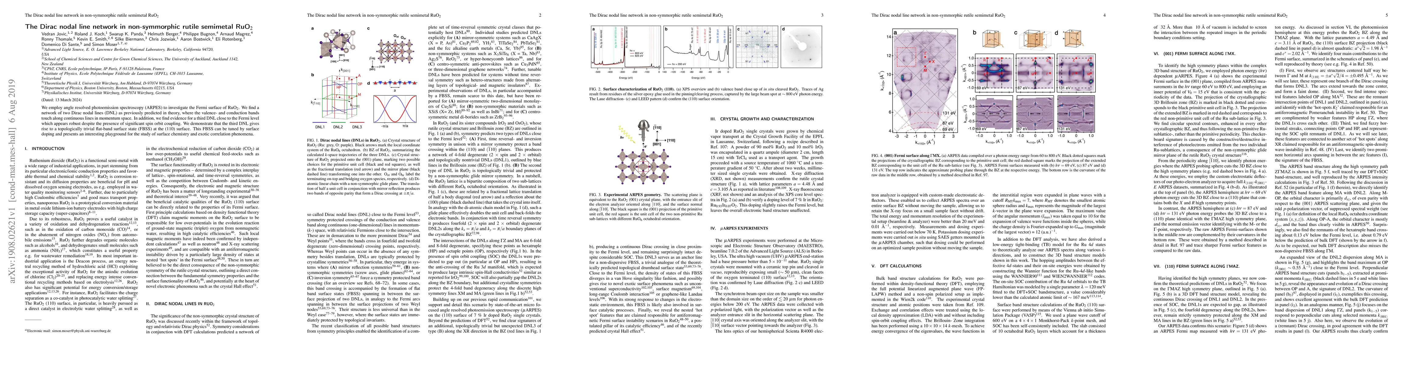
We employ angle resolved photoemission spectroscopy (ARPES) to investigate the Fermi surface of RuO$_2$. We find a network of two Dirac nodal lines (DNL) as previously predicted in theory, where the...
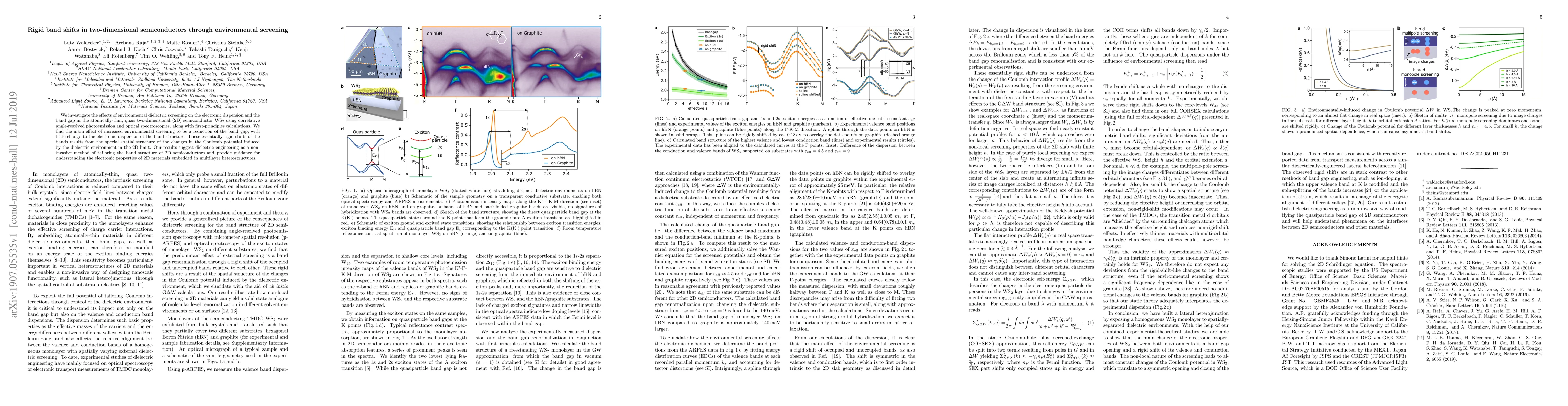
We investigate the effects of environmental dielectric screening on the electronic dispersion and the band gap in the atomically-thin, quasi two-dimensional (2D) semiconductor WS$_2$ using correlati...
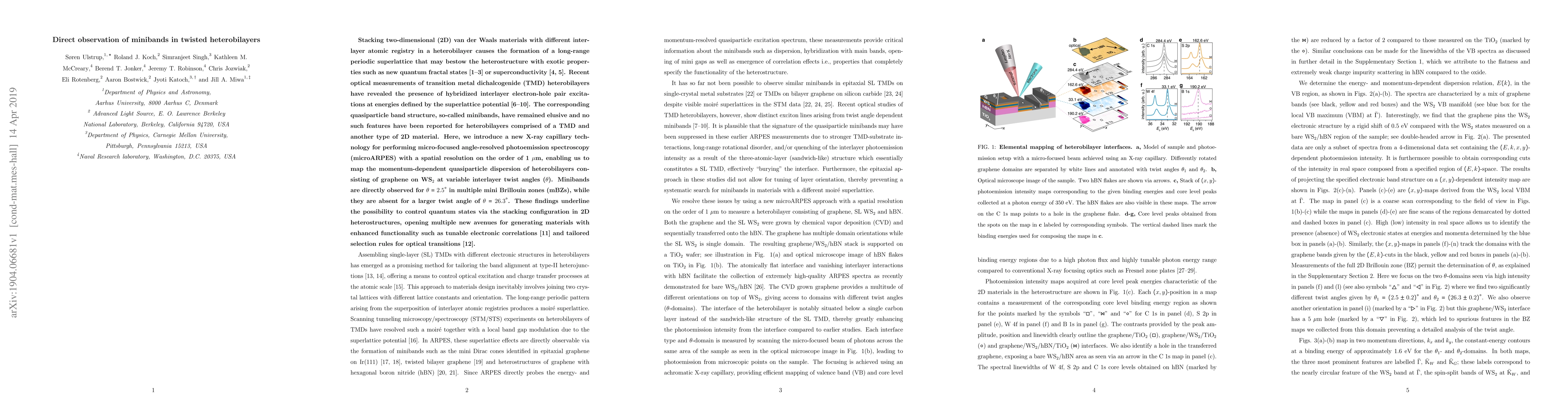
Stacking two-dimensional (2D) van der Waals materials with different interlayer atomic registry in a heterobilayer causes the formation of a long-range periodic superlattice that may bestow the hete...
The electronic properties of devices based on two-dimensional materials are significantly influenced by interactions with substrate and electrode materials. Here, we use photoemission electron micro...