Rigid band shifts in two-dimensional semiconductors through environmental screening
Publication
Metrics
AI Quick Summary
This study examines how environmental dielectric screening impacts the electronic properties of WS$_2$, a quasi-two-dimensional semiconductor, revealing that increased screening primarily reduces the band gap while minimally altering electronic dispersion. These rigid band shifts are attributed to the unique spatial structure of the dielectric-induced Coulomb potential changes.
Paper Preview
Abstract
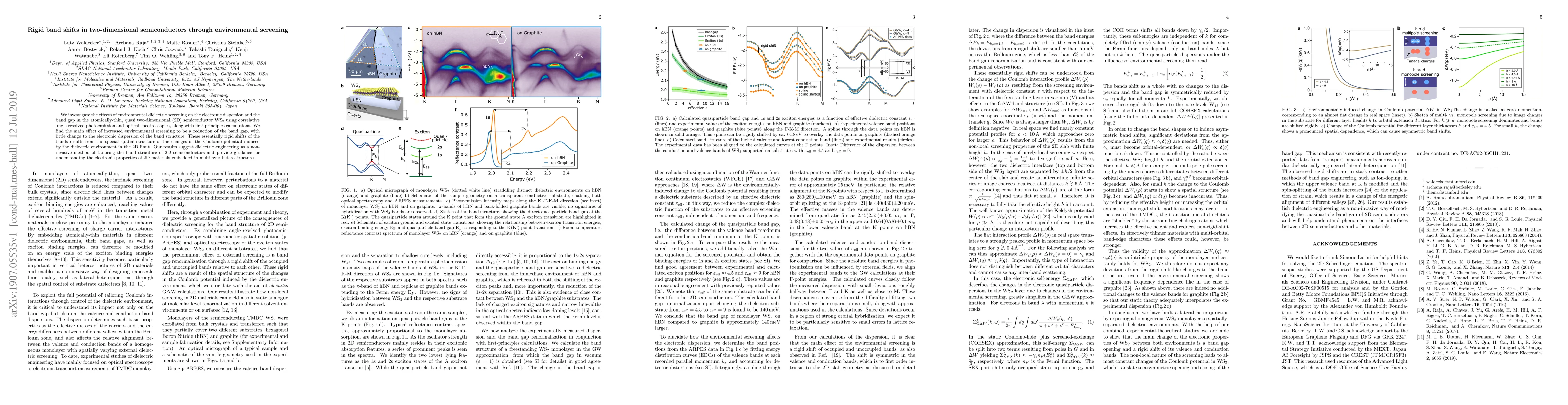
We investigate the effects of environmental dielectric screening on the electronic dispersion and the band gap in the atomically-thin, quasi two-dimensional (2D) semiconductor WS$_2$ using correlative angle-resolved photoemission and optical spectroscopies, along with first-principles calculations. We find the main effect of increased environmental screening to be a reduction of the band gap, with little change to the electronic dispersion of the band structure. These essentially rigid shifts of the bands results from the special spatial structure of the changes in the Coulomb potential induced by the dielectric environment in the 2D limit. Our results suggest dielectric engineering as a non-invasive method of tailoring the band structure of 2D semiconductors and provide guidance for understanding the electronic properties of 2D materials embedded in multilayer heterostructures.
AI Key Findings
Get AI-generated insights about this paper's methodology, results, significance, and more — seven facets brought into focus.
Impact
Paper Details
Authors
PDF Preview
Key Terms
Citation Network
Current paper (gray), citations (green), references (blue)
Display is limited for performance on very large graphs.
Discussion 0