Academic Profile
Statistics
Similar Authors
Papers on arXiv
Kagome vanadates {\it A}V$_3$Sb$_5$ display unusual low-temperature electronic properties including charge density waves (CDW), whose microscopic origin remains unsettled. Recently, CDW order has be...
Many people have flipped coins but few have stopped to ponder the statistical and physical intricacies of the process. In a preregistered study we collected $350{,}757$ coin flips to test the counte...
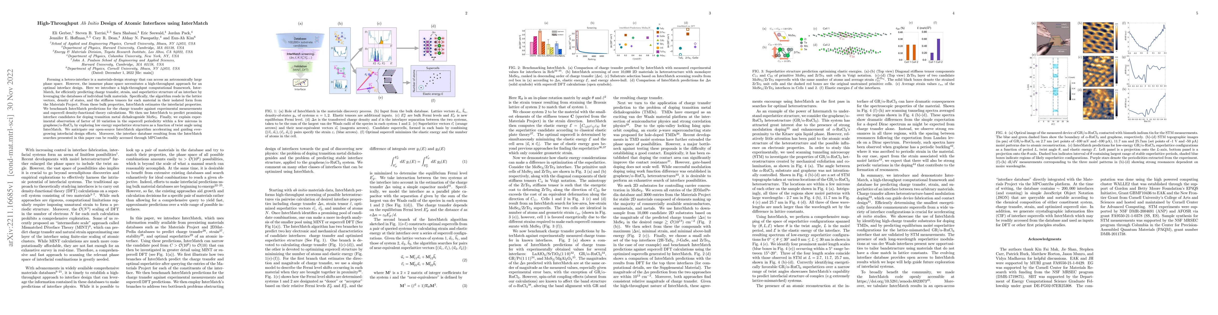
Forming a hetero-interface is a materials-design strategy that can access an astronomically large phase space. However, the immense phase space necessitates a high-throughput approach for optimal in...
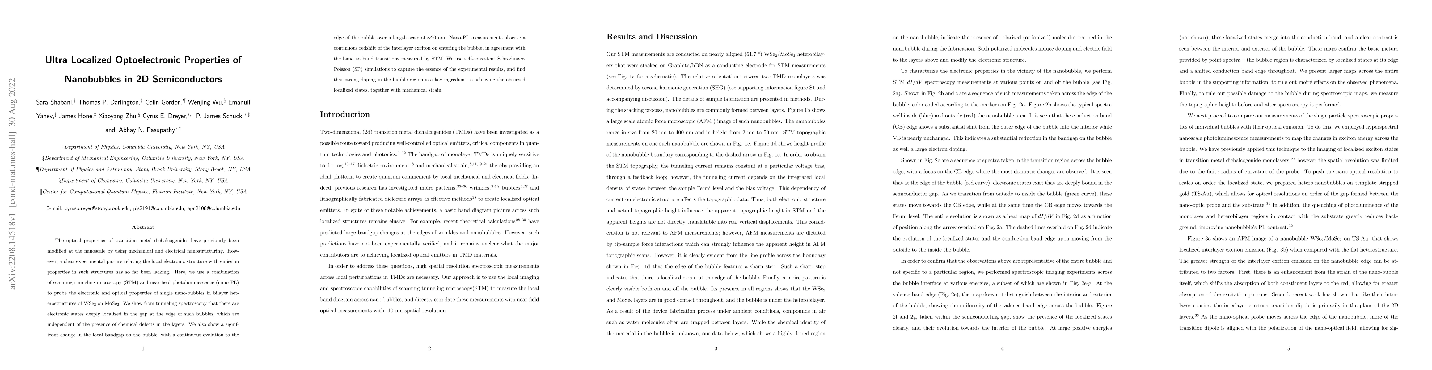
The optical properties of transition metal dichalcogenides have previously been modified at the nanoscale by using mechanical and electrical nanostructuring. However, a clear experimental picture re...
Electron-lattice coupling effects in low dimensional materials give rise to charge density wave (CDW) order and phase transitions. These phenomena are critical ingredients for superconductivity and ...
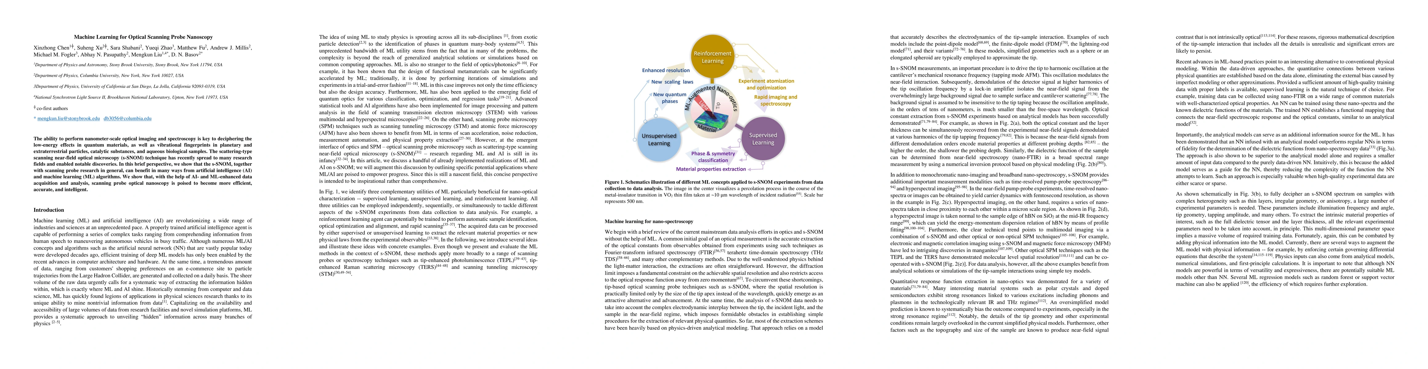
The ability to perform nanometer-scale optical imaging and spectroscopy is key to deciphering the low-energy effects in quantum materials, as well as vibrational fingerprints in planetary and extrat...
The ability to create high-quality lateral p-n junctions at nanometer length scales is essential for the next generation of two-dimensional (2D) electronic and plasmonic devices. Using a charge-tran...
Deep learning (DL) is an emerging analysis tool across sciences and engineering. Encouraged by the successes of DL in revealing quantitative trends in massive imaging data, we applied this approach ...
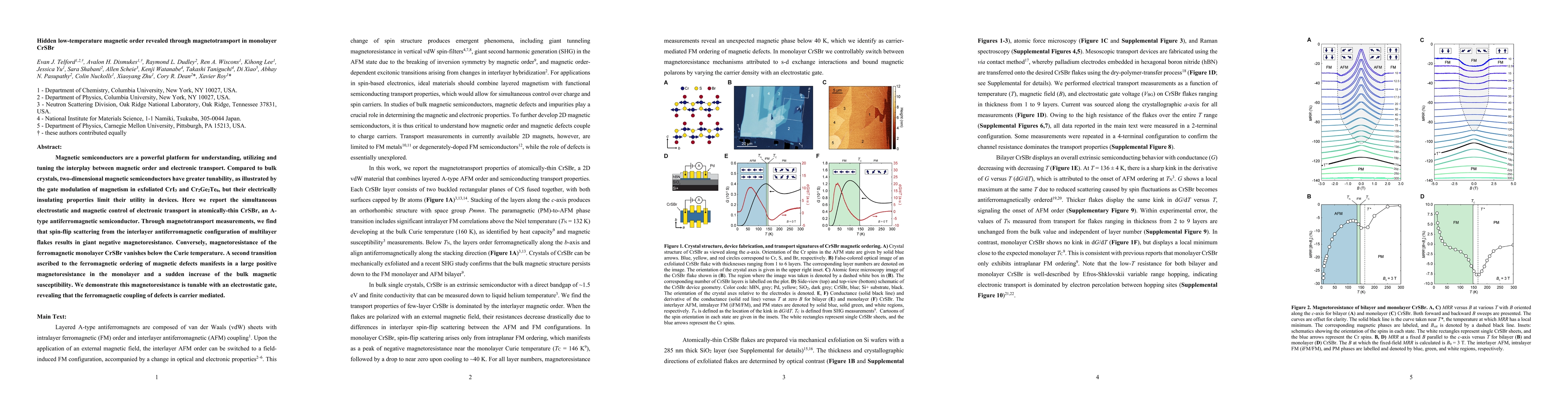
Magnetic semiconductors are a powerful platform for understanding, utilizing and tuning the interplay between magnetic order and electronic transport. Compared to bulk crystals, two-dimensional magn...
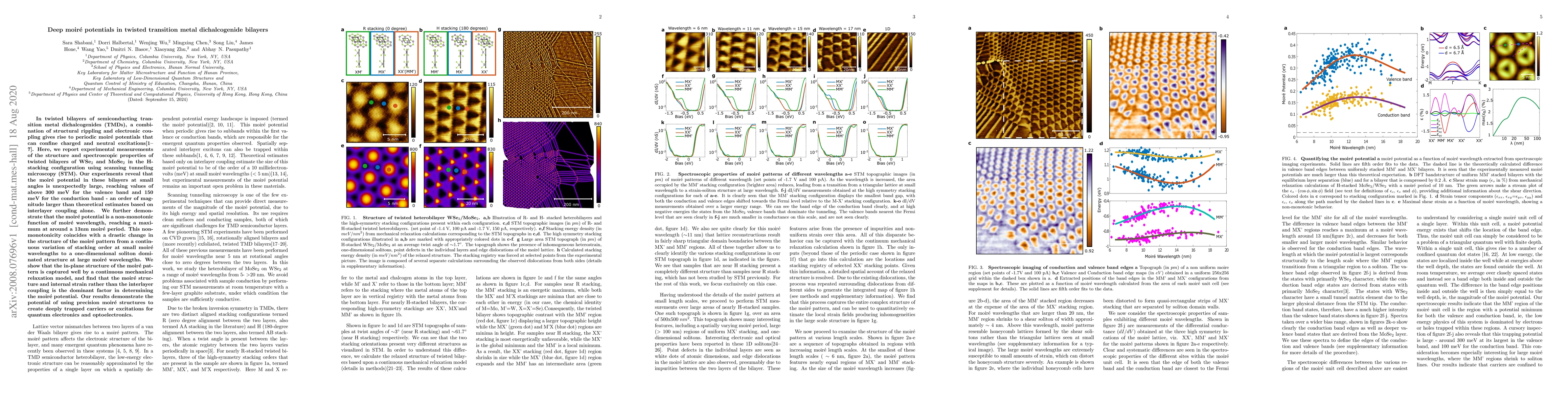
In twisted bilayers of semiconducting transition metal dichalcogenides (TMDs), a combination of structural rippling and electronic coupling gives rise to periodic moir\'e potentials that can confine...
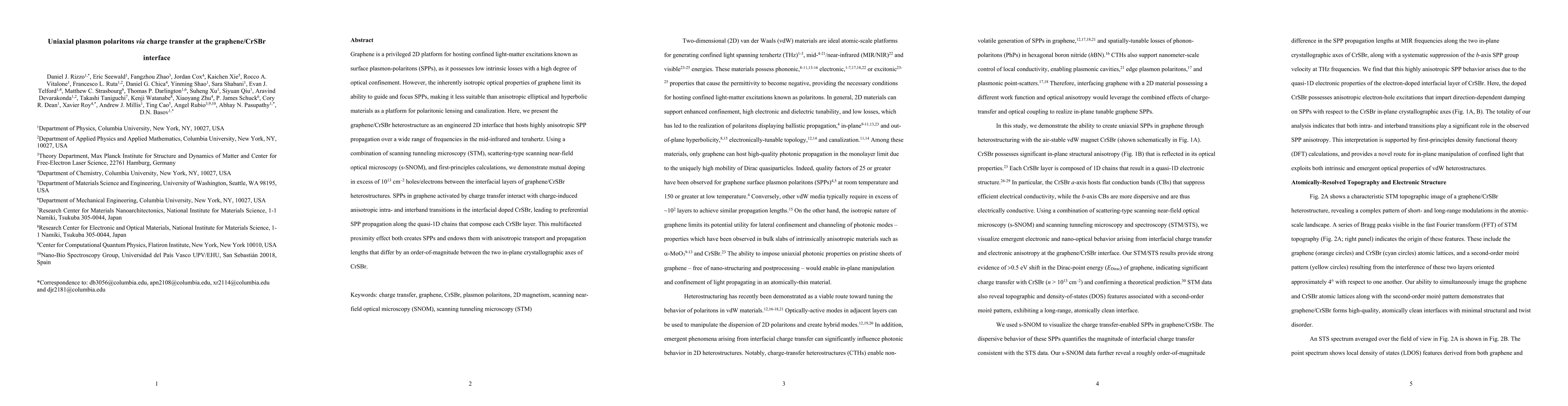
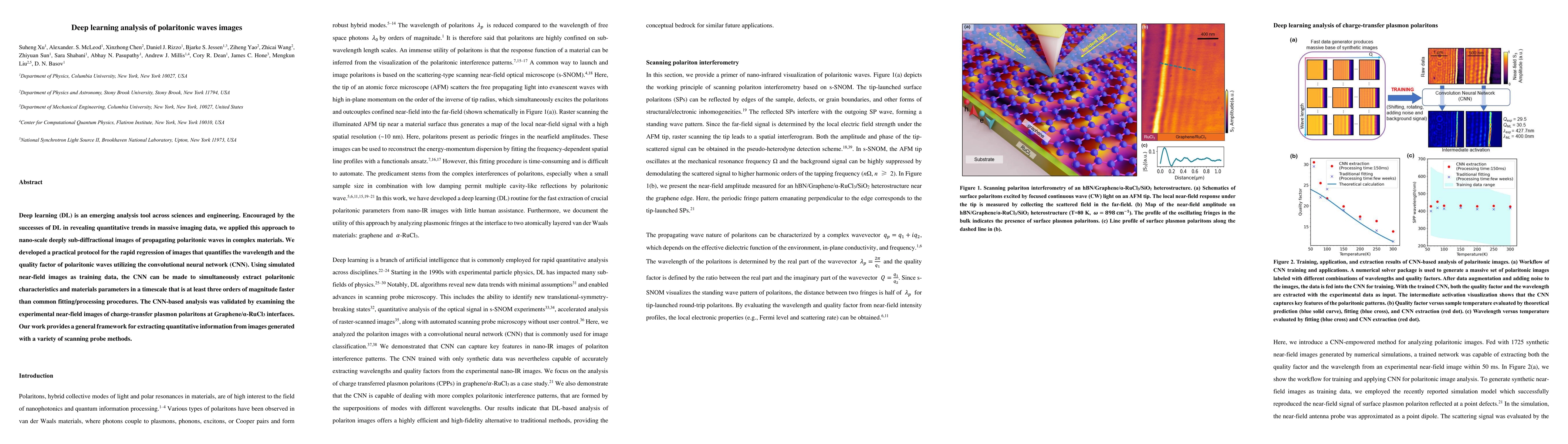
Graphene is a privileged 2D platform for hosting confined light-matter excitations known as surface plasmon-polaritons (SPPs), as it possesses low intrinsic losses with a high degree of optical confin...
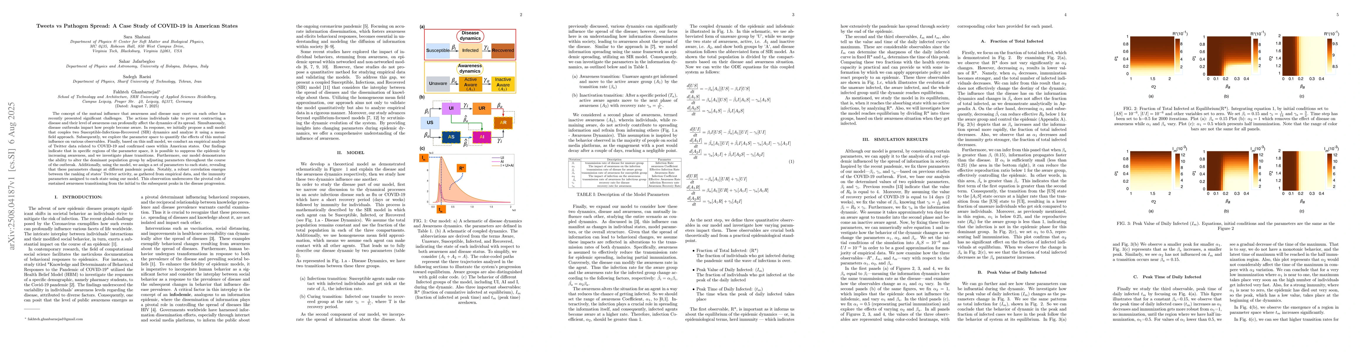
The concept of the mutual influence that awareness and disease may exert on each other has recently presented significant challenges. The actions individuals take to prevent contracting a disease and ...
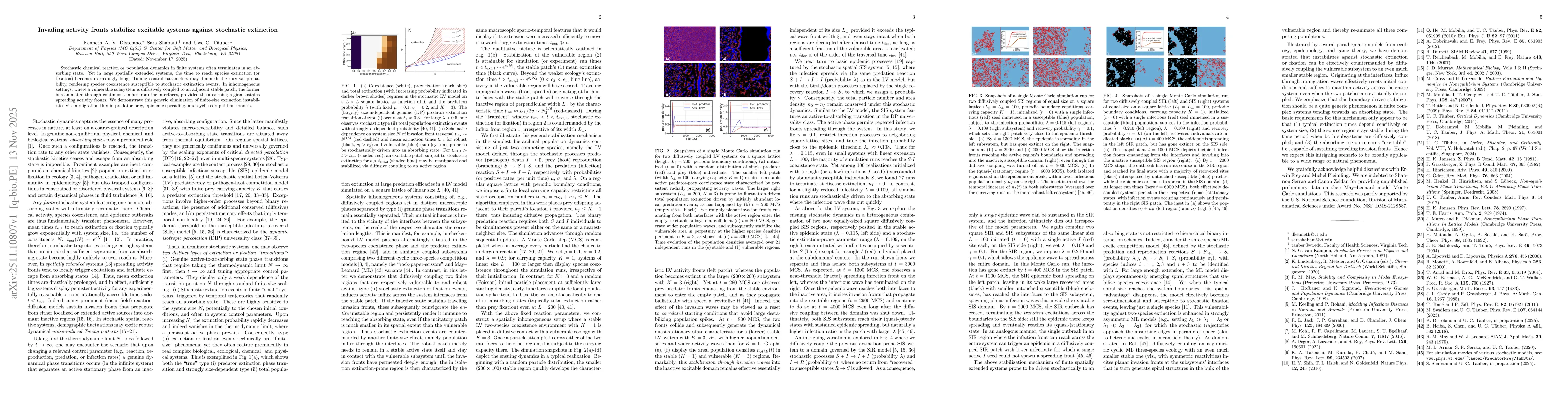
Stochastic chemical reaction or population dynamics in finite systems often terminates in an absorbing state. Yet in large spatially extended systems, the time to reach species extinction (or fixation...