1
arXiv Papers
14
Total Publications
Profile
Academic Profile
Metrics
Statistics
1
arXiv Papers
14
Total Publications
Network
Similar Authors
Publications
Papers on arXiv
arXiv
Automated high-resolution backscattered-electron imaging at macroscopic
scale
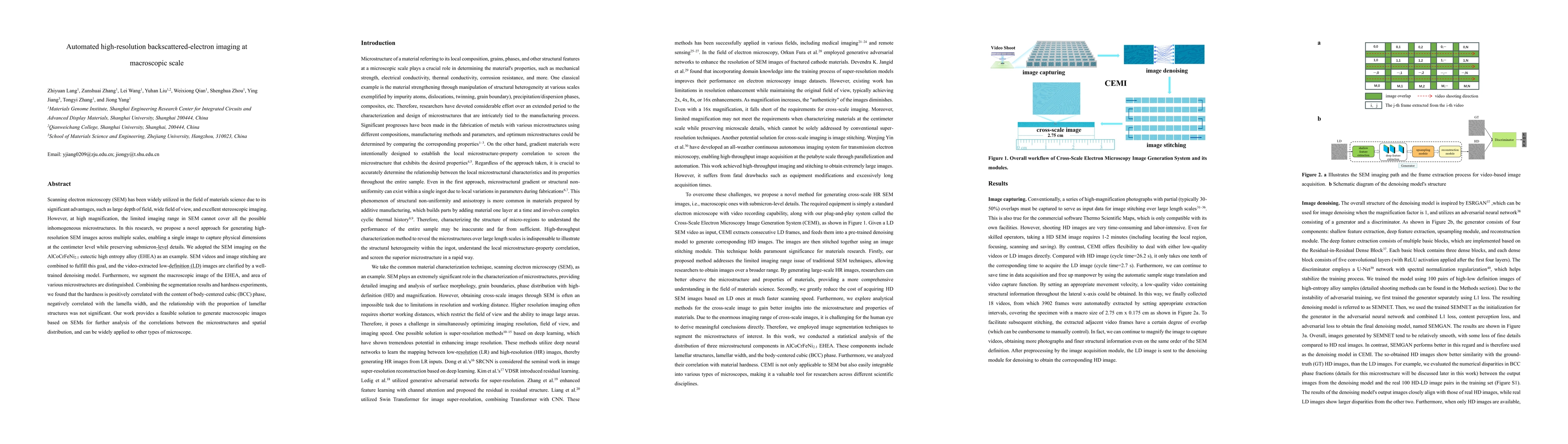
Scanning electron microscopy (SEM) has been widely utilized in the field of materials science due to its significant advantages, such as large depth of field, wide field of view, and excellent stereos...