Academic Profile
Statistics
Similar Authors
Papers on arXiv
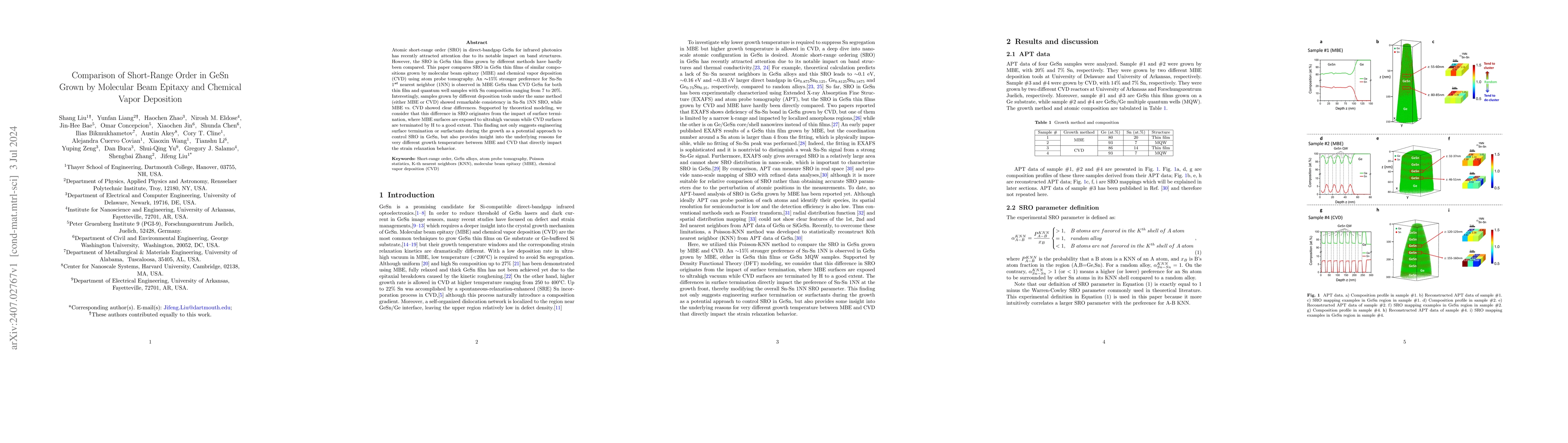
Atomic short-range order (SRO) in direct-bandgap GeSn for infrared photonics has recently attracted attention due to its notable impact on band structures. However, the SRO in GeSn thin films grown ...
We demonstrate monolithically grown germanium-tin (GeSn) on silicon avalanche photodiodes (APDs) for infrared light detection. A relatively thinner Ge buffer design was adopted to allow effective ph...
Owing to its true direct bandgap and tunable bandgap energies,GeSn alloys are increasingly attractive as gain media for mid-IR lasers that can be monolithically integrated on Si. Demonstrations of o...
GeSn on Si has attracted much research interest due to its tunable direct bandgap for mid-infrared applications. Recently, short-range order (SRO) in GeSn alloys has been theoretically predicted, wh...
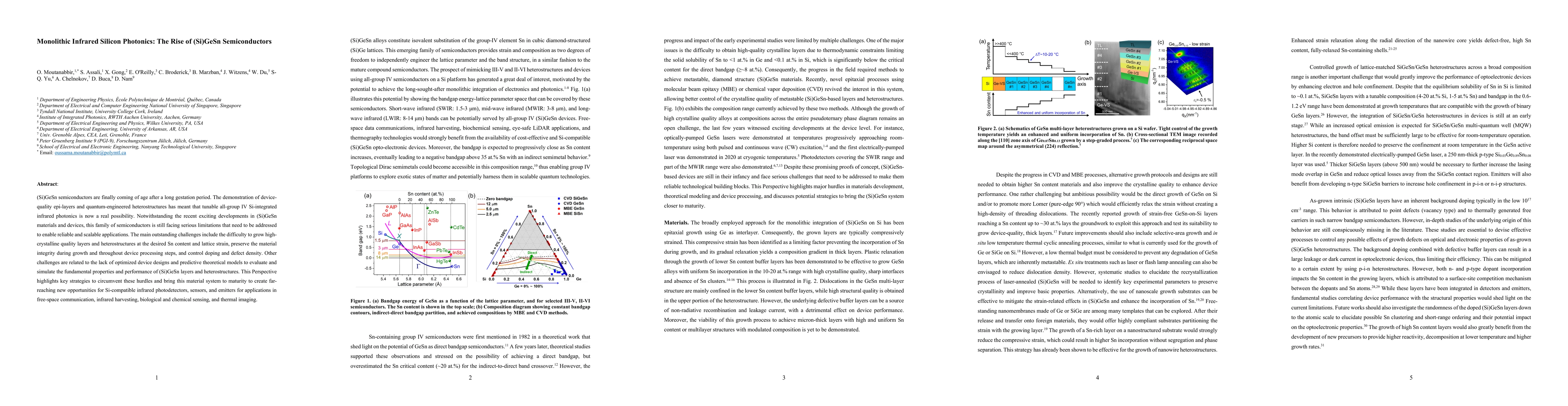
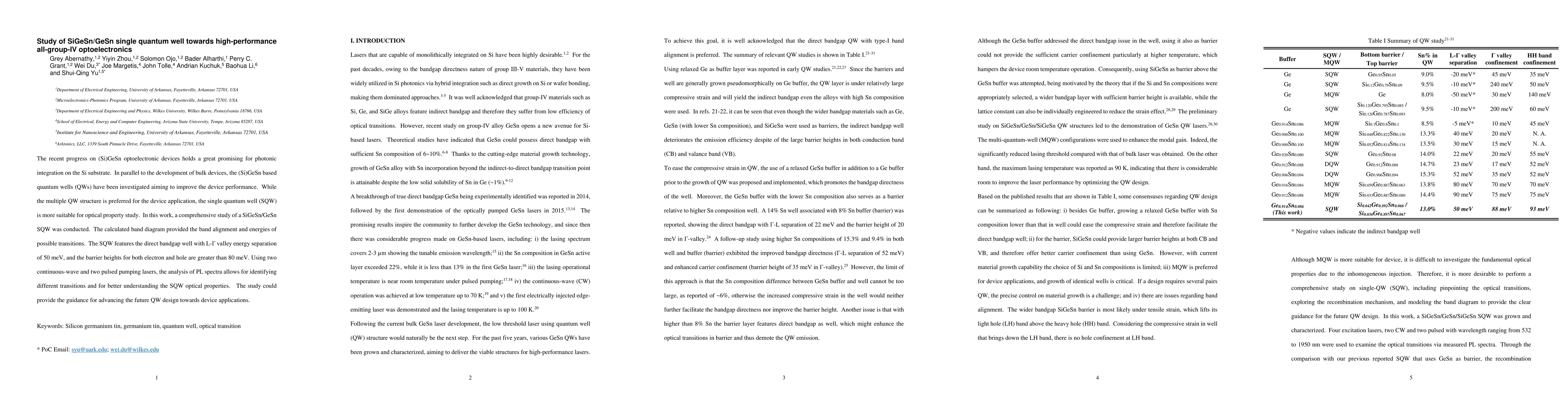
(Si)GeSn semiconductors are finally coming of age after a long gestation period. The demonstration of device quality epi-layers and quantum-engineered heterostructures has meant that tunable all-gro...
The recent progress on (Si)GeSn optoelectronic devices holds a great promising for photonic integration on the Si substrate. In parallel to the development of bulk devices, the (Si)GeSn based quantu...
GeSn lasers enable monolithic integration of lasers on the Si platform using all-group-IV direct-bandgap materials. Although optically pumped GeSn lasers have made significant progress, the study of...
The significant progress of GeSn material development has enabled a feasible solution to the long-desired monolithically integrated lasers on the Si platform. While there are many reports focused on...
This paper reports a comprehensive study of Si-based GeSn mid-infrared photodetectors, which includes: 1) the demonstration of a set of photoconductors with Sn compositions ranging from 10.5% to 22....
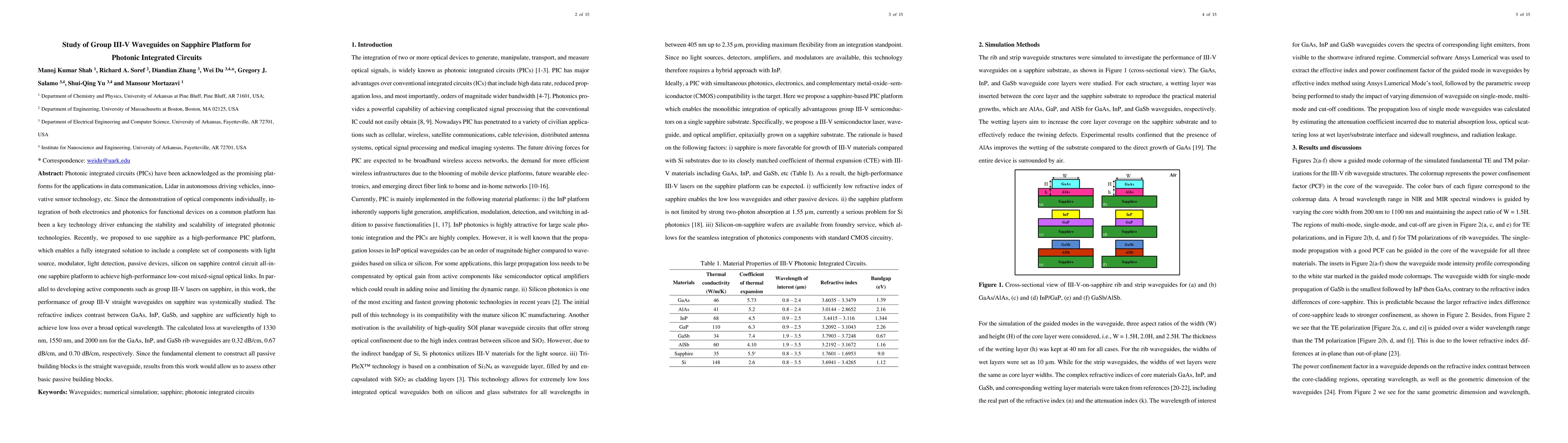
Photonic integrated circuits (PICs) have been acknowledged as the promising platforms for the applications in data communication, Lidar in autonomous driving vehicles, innovative sensor technology, et...
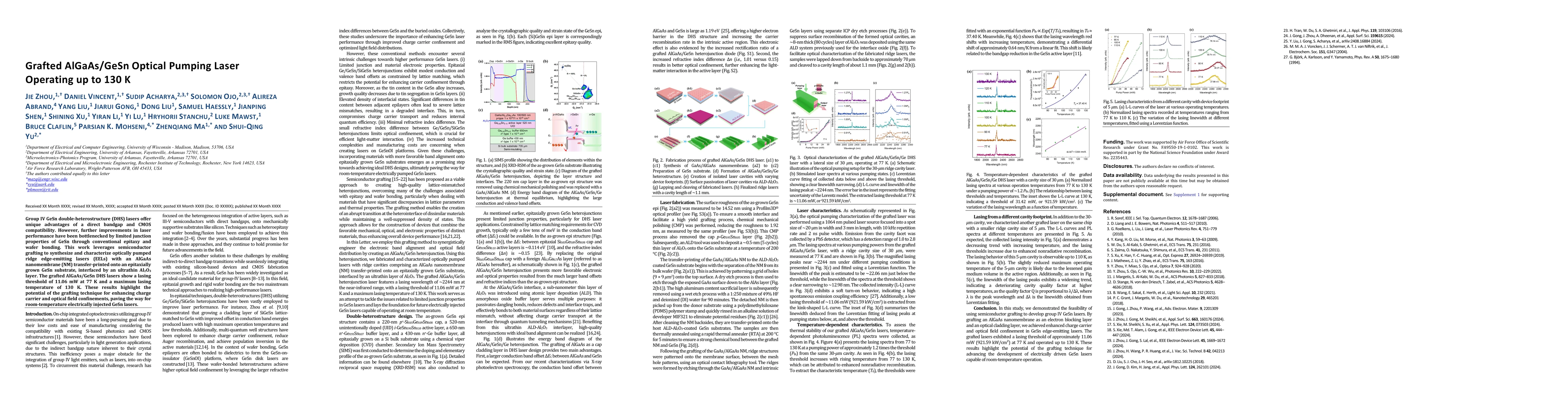
Group IV GeSn double-heterostructure (DHS) lasers offer unique advantages of a direct bandgap and CMOS compatibility. However, further improvements in laser performance have been bottlenecked by limit...
GeSn-based SWIR lasers featuring imaging, sensing, and communications has gained dynamic development recently. However, the existing SiGeSn/GeSn double heterostructure lacks adequate electron confinem...
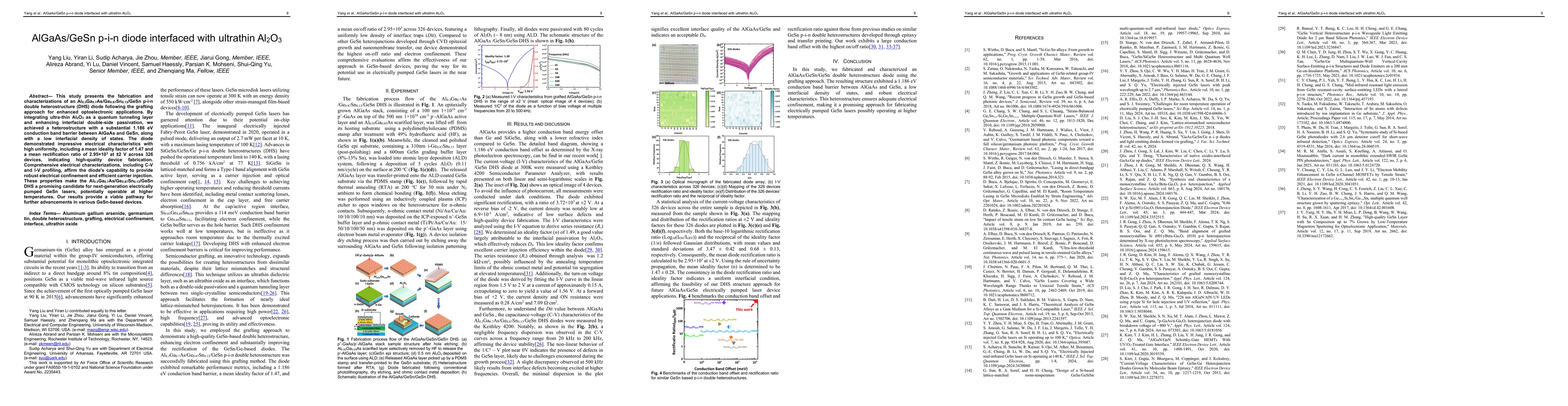
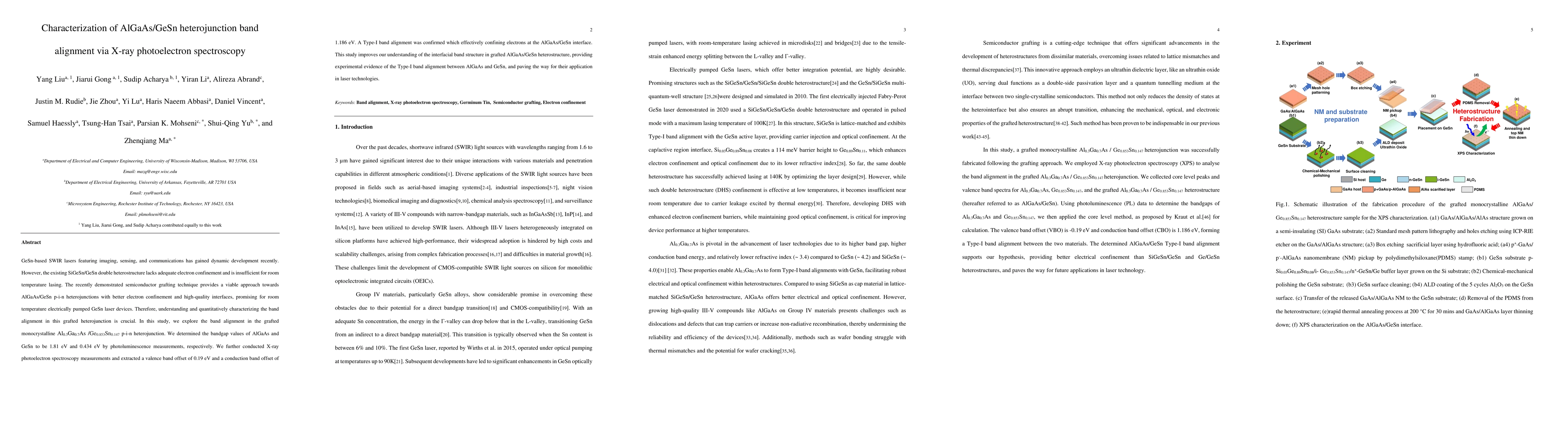
This study presents the fabrication and characterizations of an Al$_{0.3}$Ga$_{0.7}$As/Ge$_{0.87}$Sn$_{0.13}$/GeSn p-i-n double heterostructure (DHS) diode following the grafting approach for enhanced...
Group IV alloys of GeSn have gained significant attention for electronic and optoelectronic applications on a Si platform due to their compatibility with existing CMOS technology, tunable band structu...
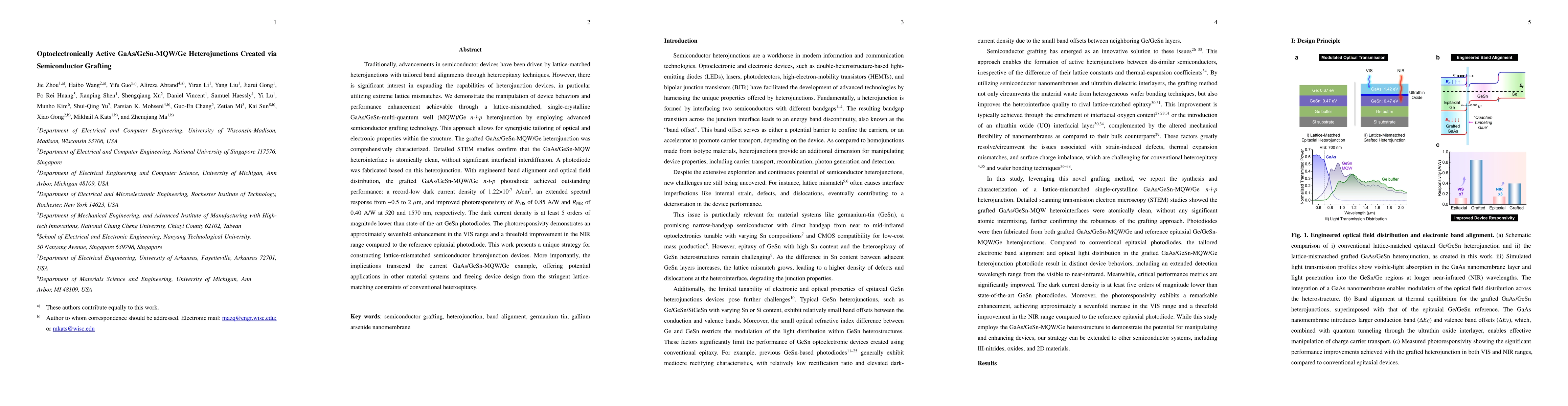
Traditionally, advancements in semiconductor devices have been driven by lattice-matched heterojunctions with tailored band alignments through heteroepitaxy techniques. However, there is significant i...
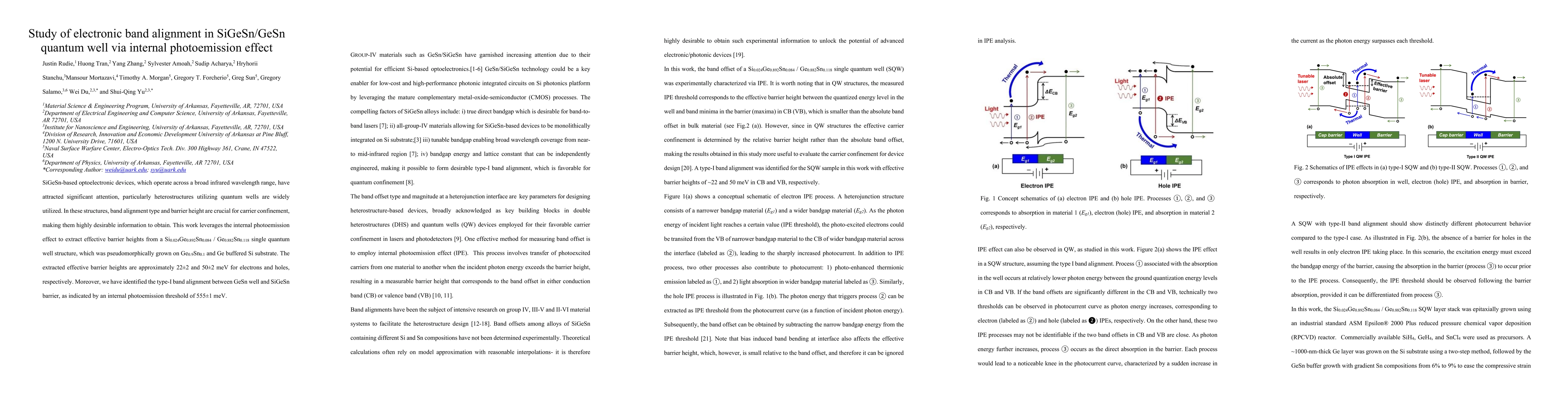
SiGeSn-based optoelectronic devices, which operate across a broad infrared wavelength range, have attracted significant attention, particularly heterostructures utilizing quantum wells are widely util...
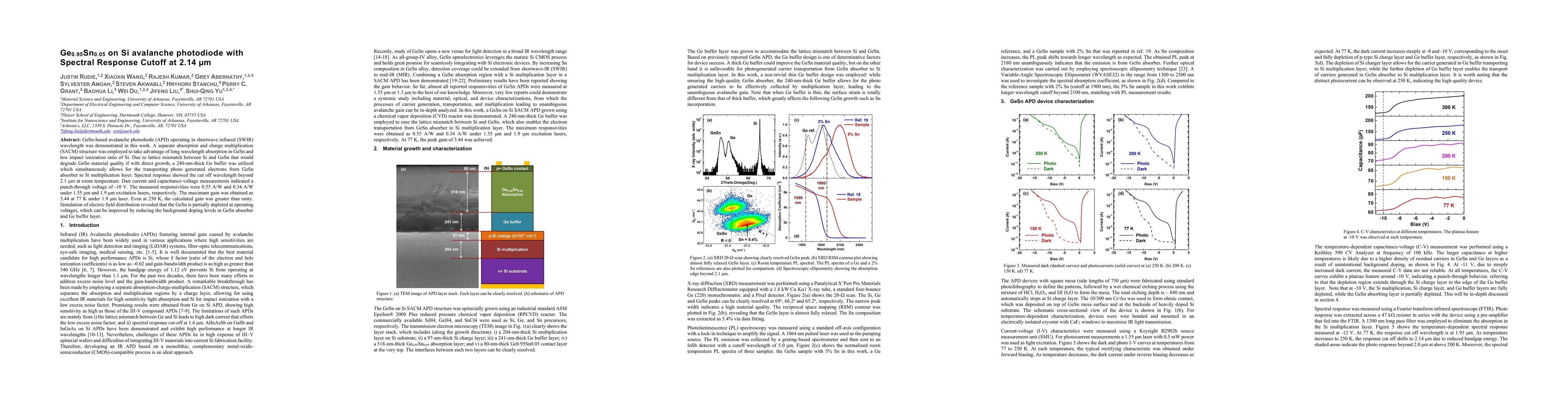
GeSn-based avalanche photodiode (APD) operating in shortwave infrared (SWIR) wavelength was demonstrated in this work. A separate absorption and charge multiplication (SACM) structure was employed to ...
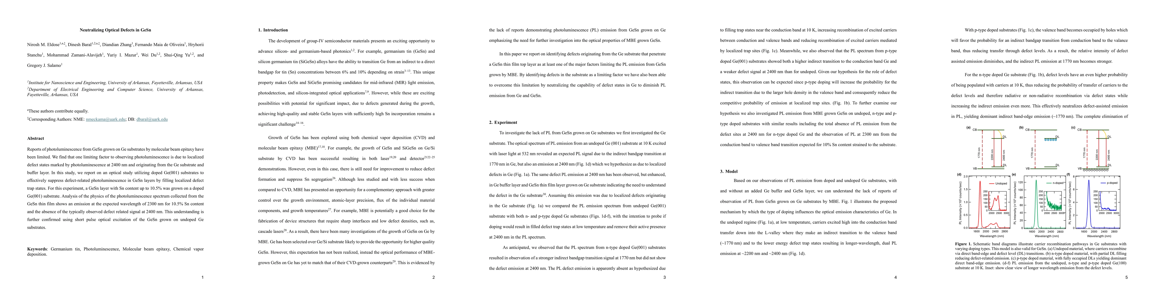
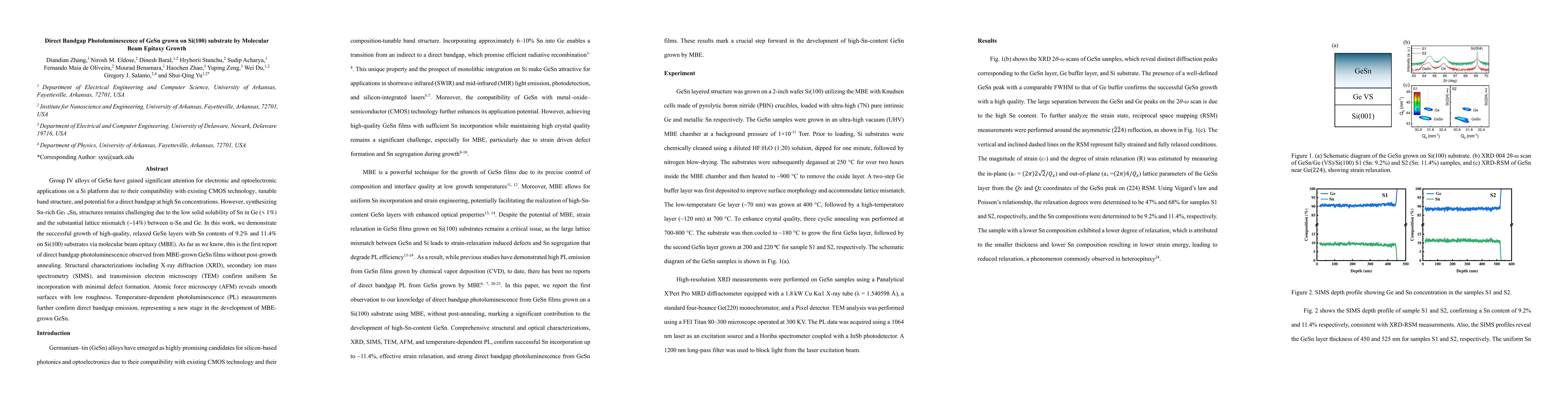
Reports of photoluminescence from GeSn grown on Ge substrates by molecular beam epitaxy have been limited. We find that one limiting factor to observing photoluminescence is due to localized defect st...
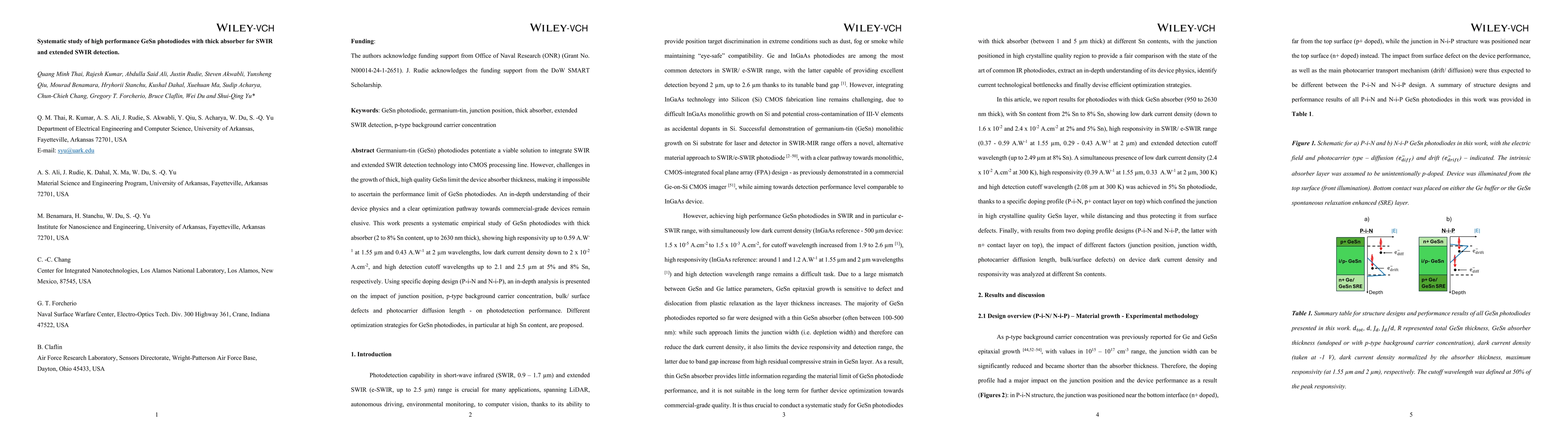
Germanium-tin (GeSn) photodiodes potentiate a viable solution to integrate SWIR and extended SWIR detection technology into CMOS processing line. However, challenges in the growth of thick, high quali...
Separate absorption charge multiplication germanium tin on silicon avalanche photodiode offers a viable solution to achieve CMOS compatible, high sensitivity detection technology in SWIR or extended S...
Hole spin qubits in germanium (Ge)-based heterostructures have demonstrated their potential for scalable quantum information processing using all-electrical gate operations. Furthermore, the emerging ...