Summary
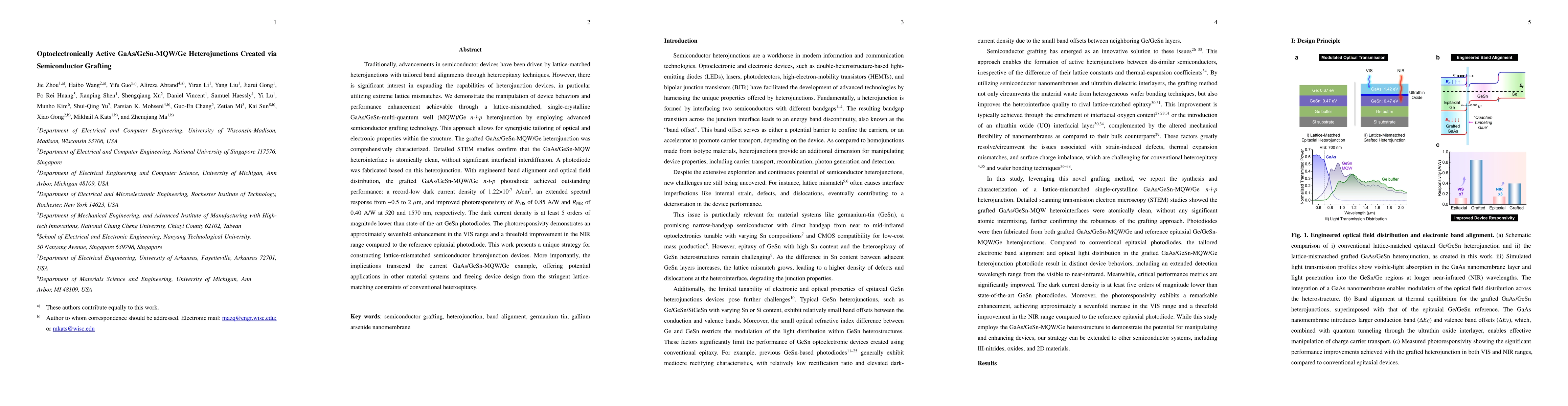
Traditionally, advancements in semiconductor devices have been driven by lattice-matched heterojunctions with tailored band alignments through heteroepitaxy techniques. However, there is significant interest in expanding the capabilities of heterojunction devices, in particular utilizing extreme lattice mismatches. We demonstrate the manipulation of device behaviors and performance enhancement achievable through a lattice-mismatched, single-crystalline GaAs/GeSn-multi-quantum well (MQW)/Ge n-i-p heterojunction by employing advanced semiconductor grafting technology. With engineered band alignment and optical field distribution, the grafted GaAs/GeSn-MQW/Ge n-i-p photodiode achieved outstanding performance: a record-low dark current density of 1.22E10^-7 A/cm^2, an extended spectral response from ~0.5 to 2 um, and improved photoresponsivity of RVIS of 0.85 A/W and RNIR of 0.40 A/W at 520 and 1570 nm, respectively. The dark current density is at least 5 orders of magnitude lower than state-of-the-art GeSn photodiodes. The photoresponsivity demonstrates an approximately sevenfold enhancement in the VIS range and a threefold improvement in the NIR range compared to the reference epitaxial photodiode. This work presents a unique strategy for constructing lattice-mismatched semiconductor heterojunction devices. More importantly, the implications transcend the current GaAs/GeSn-MQW/Ge example, offering potential applications in other material systems and freeing device design from the stringent lattice-matching constraints of conventional heteroepitaxy.
AI Key Findings
Generated Sep 03, 2025
Methodology
The research utilized semiconductor grafting technology to create a lattice-mismatched GaAs/GeSn-MQW/Ge heterojunction, demonstrating its effectiveness through advanced characterization techniques such as XRD, STEM, and photodiode fabrication.
Key Results
- Achieved a record-low dark current density of 1.22E-7 A/cm^2 in a photodiode.
- Extended spectral response from ~0.5 to 2 µm.
- Improved photoresponsivity with RVIS of 0.85 A/W and RNIR of 0.40 A/W.
- Demonstrated dual-mode operation with VIS response at negative bias and NIR response at positive bias.
- Showed a significant reduction in dark current compared to state-of-the-art GeSn photodiodes.
Significance
This work presents a novel strategy for constructing lattice-mismatched semiconductor heterojunction devices, transcending current constraints of conventional heteroepitaxy and offering potential applications in various material systems.
Technical Contribution
The research introduced a semiconductor grafting technique to engineer band alignment and optical absorption within heterostructures, leading to enhanced photodiode performance.
Novelty
The study breaks new ground by demonstrating the feasibility and effectiveness of semiconductor grafting for creating high-performance, lattice-mismatched heterojunction devices, which was previously challenging with conventional heteroepitaxy methods.
Limitations
- The study was limited to a specific heterojunction structure (GaAs/GeSn-MQW/Ge).
- Further research is needed to validate the approach across a broader range of material systems.
Future Work
- Explore the applicability of this grafting method in other semiconductor material systems.
- Investigate the long-term stability and reliability of these grafted heterojunction devices.
Paper Details
PDF Preview
Citation Network
Current paper (gray), citations (green), references (blue)
Display is limited for performance on very large graphs.
Similar Papers
Found 4 papersWafer-scale Semiconductor Grafting: Enabling High-Performance, Lattice-Mismatched Heterojunctions
Yang Liu, Wei Lin, Jie Zhou et al.
Characterization of AlGaAs/GeSn heterojunction band alignment via X-ray photoelectron spectroscopy
Yang Liu, Jie Zhou, Shui-Qing Yu et al.
No citations found for this paper.
Comments (0)