Academic Profile
Statistics
Similar Authors
Papers on arXiv
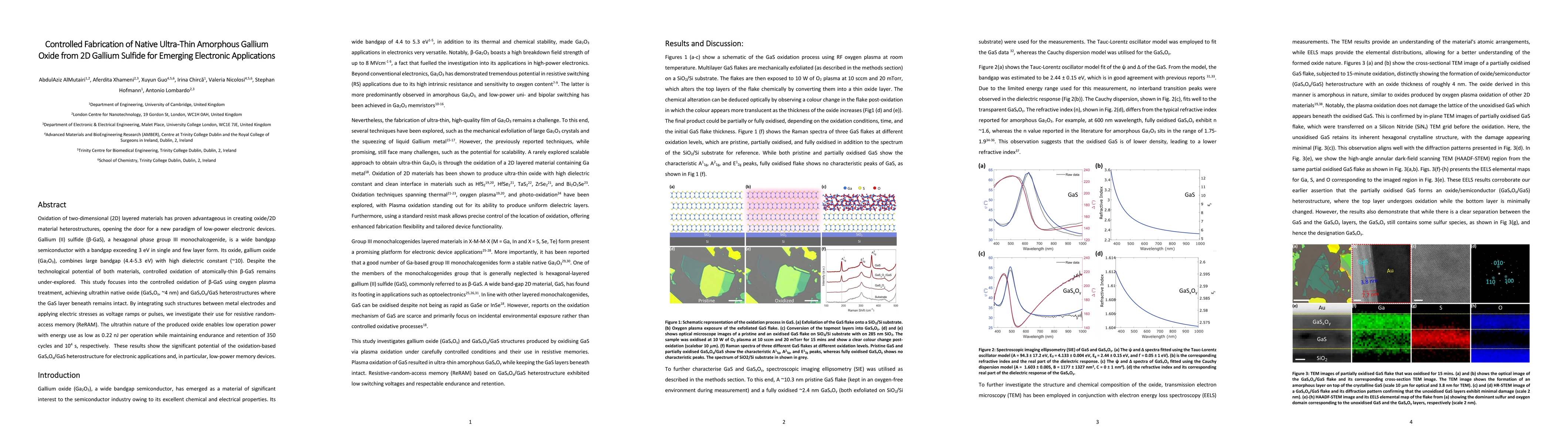
Oxidation of two-dimensional (2D) layered materials has proven advantageous in creating oxide/2D material heterostructures, opening the door for a new paradigm of low-power electronic devices. Galli...
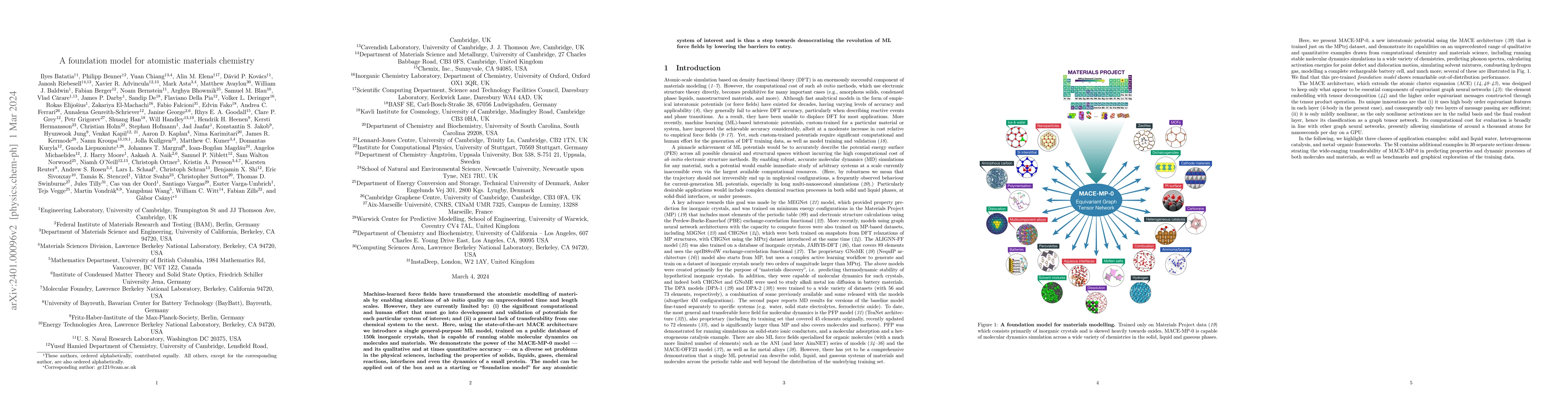
Machine-learned force fields have transformed the atomistic modelling of materials by enabling simulations of ab initio quality on unprecedented time and length scales. However, they are currently l...
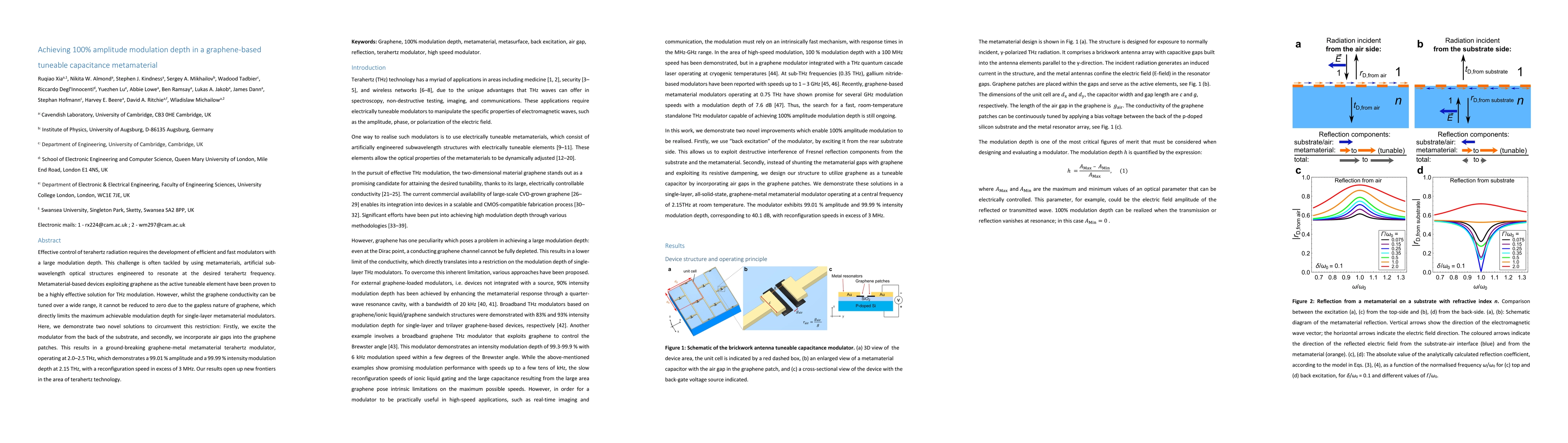
Effective control of terahertz radiation requires the development of efficient and fast modulators with a large modulation depth. This challenge is often tackled by using metamaterials, artificial s...
The role and impact of spatial heterogeneity in two-dimensional quantum materials represents one of the major research quests regarding the future application of these materials in optoelectronics a...
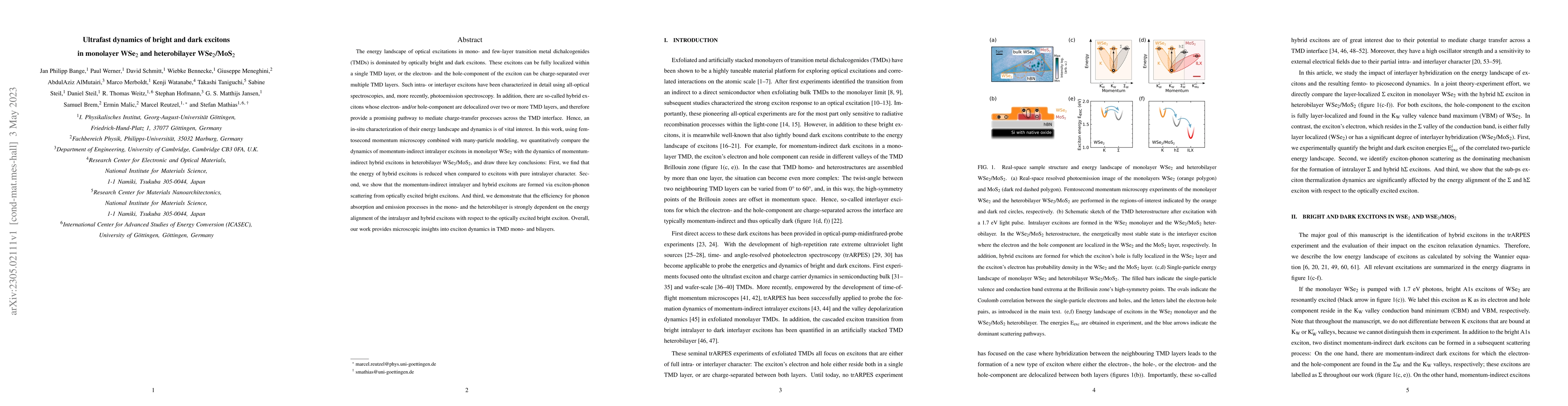
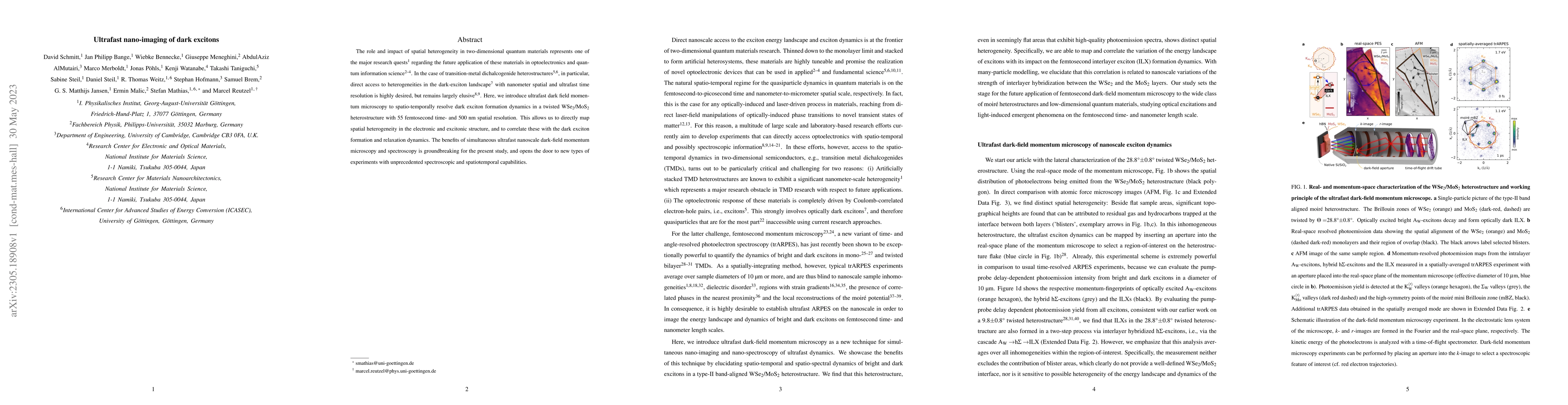
The energy landscape of optical excitations in mono- and few-layer transition metal dichalcogenides (TMDs) is dominated by optically bright and dark excitons. These excitons can be fully localized w...
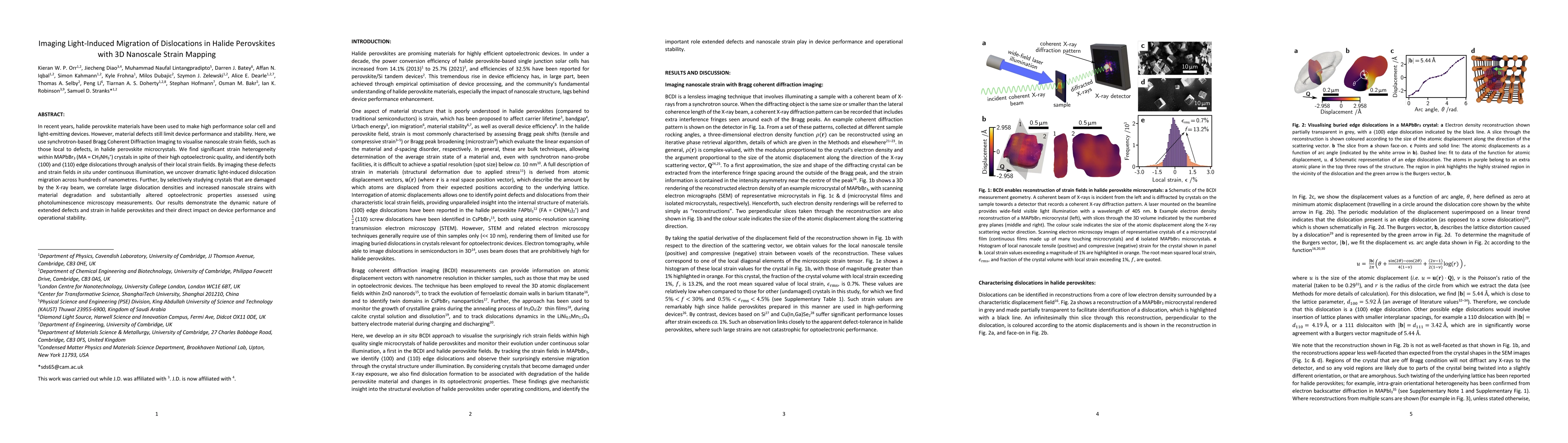
In recent years, halide perovskite materials have been used to make high performance solar cell and light-emitting devices. However, material defects still limit device performance and stability. He...
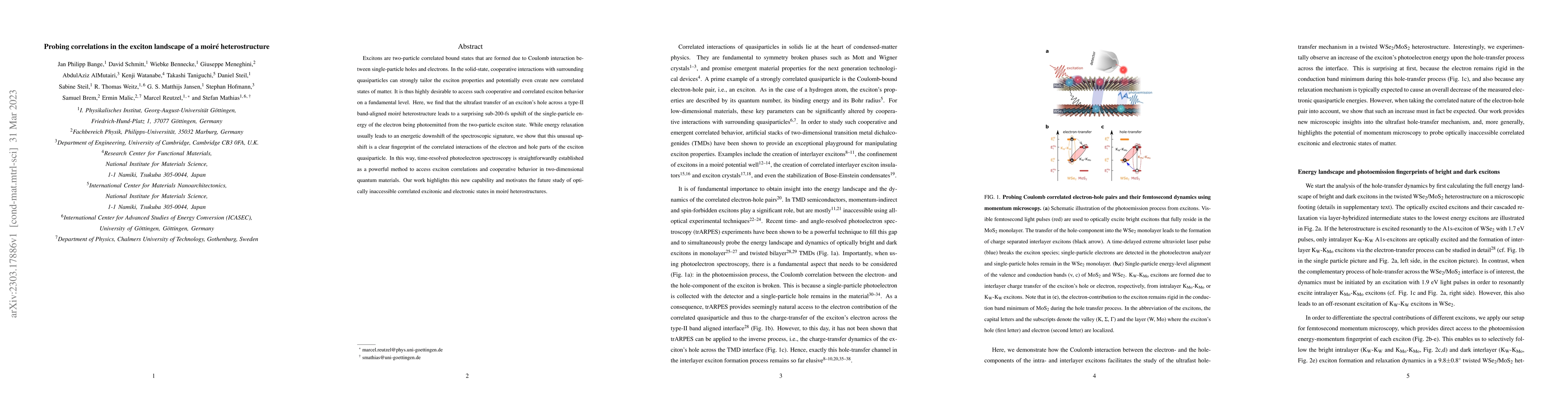
Excitons are two-particle correlated bound states that are formed due to Coulomb interaction between single-particle holes and electrons. In the solid-state, cooperative interactions with surroundin...
Identification of non-amplified DNA sequences and single-base mutations is essential for molecular biology and genetic diagnostics. This paper reports a novel sensor consisting of electrochemically-...
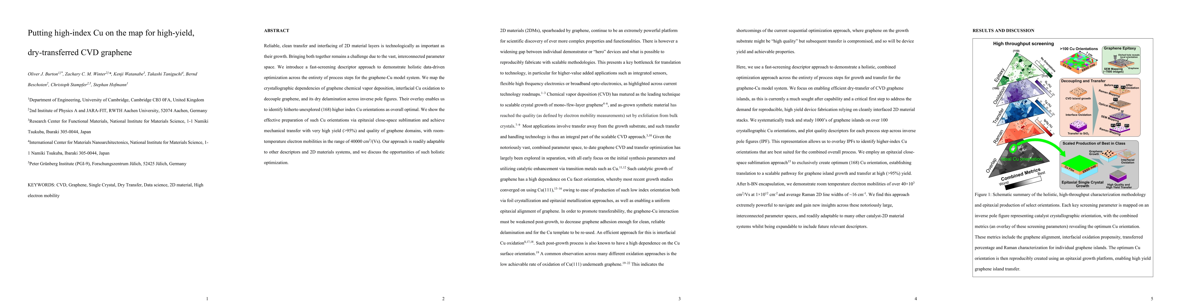
Reliable, clean transfer and interfacing of 2D material layers is technologically as important as their growth. Bringing both together remains a challenge due to the vast, interconnected parameter s...
The deposition of dielectric materials on graphene is one of the bottlenecks for unlocking the potential of graphene in electronic applications. In this paper we demonstrate the plasma enhanced atom...
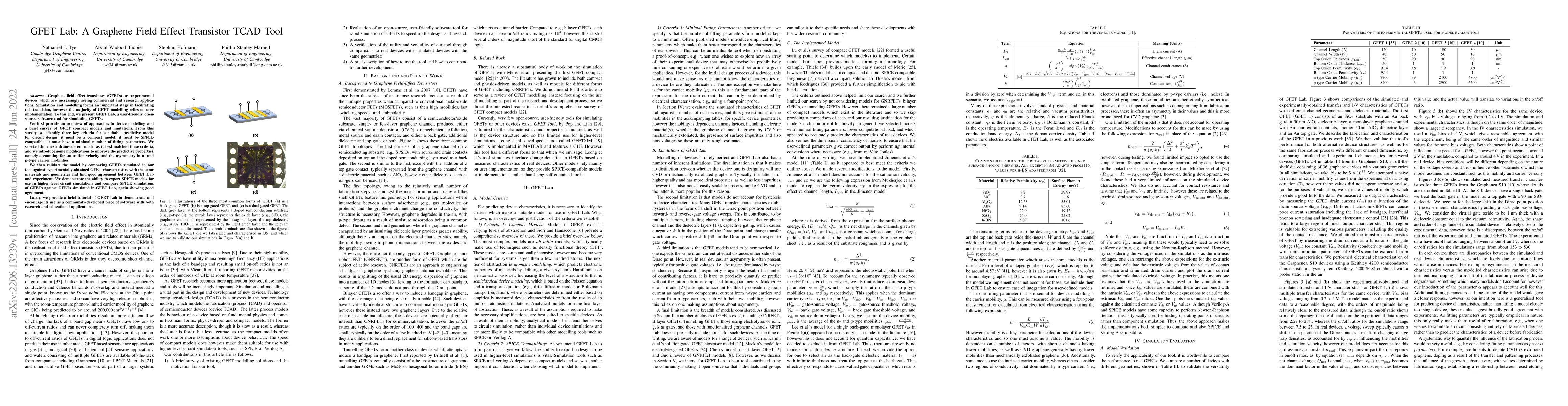
Graphene field-effect transistors (GFETs) are experimental devices which are increasingly seeing commercial and research applications. Simulation and modelling forms an important stage in facilitati...
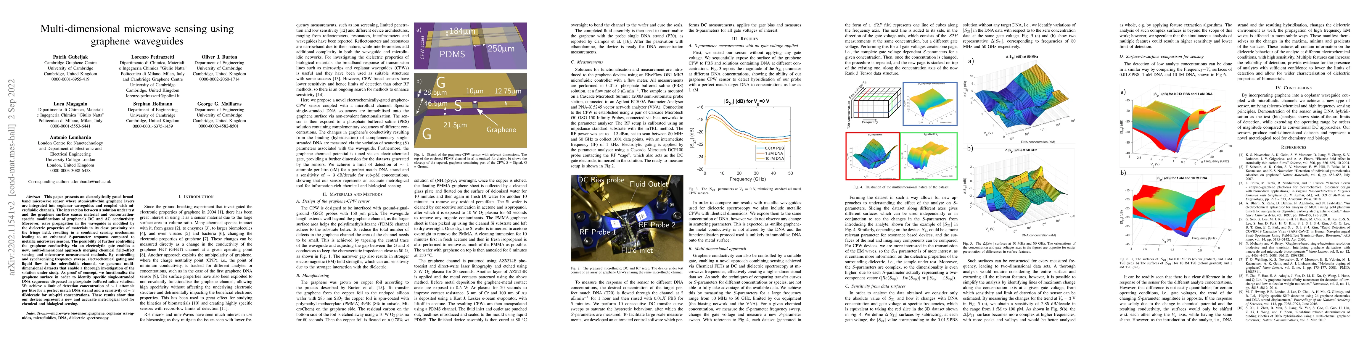
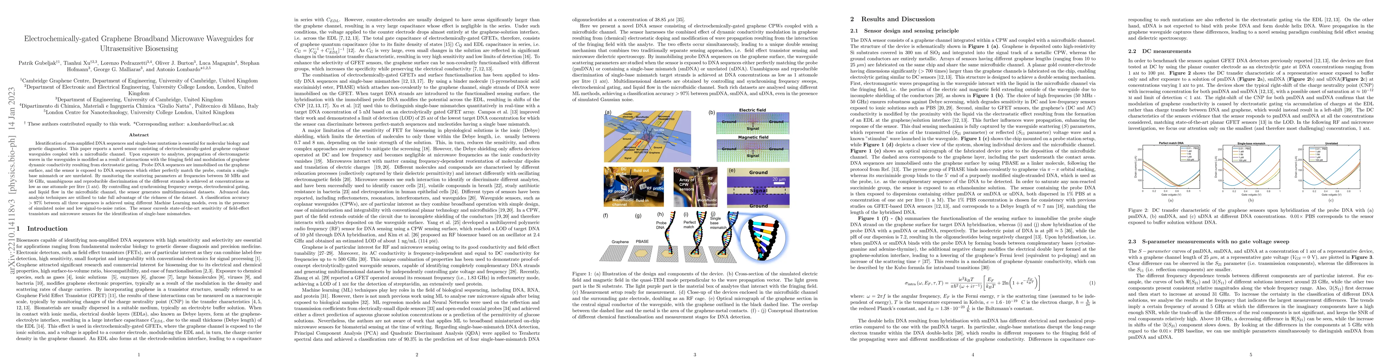
This paper presents an electrolytically gated broadband microwave sensor where atomically-thin graphene layers are integrated into coplanar waveguides and coupled with microfluidic channels. The int...
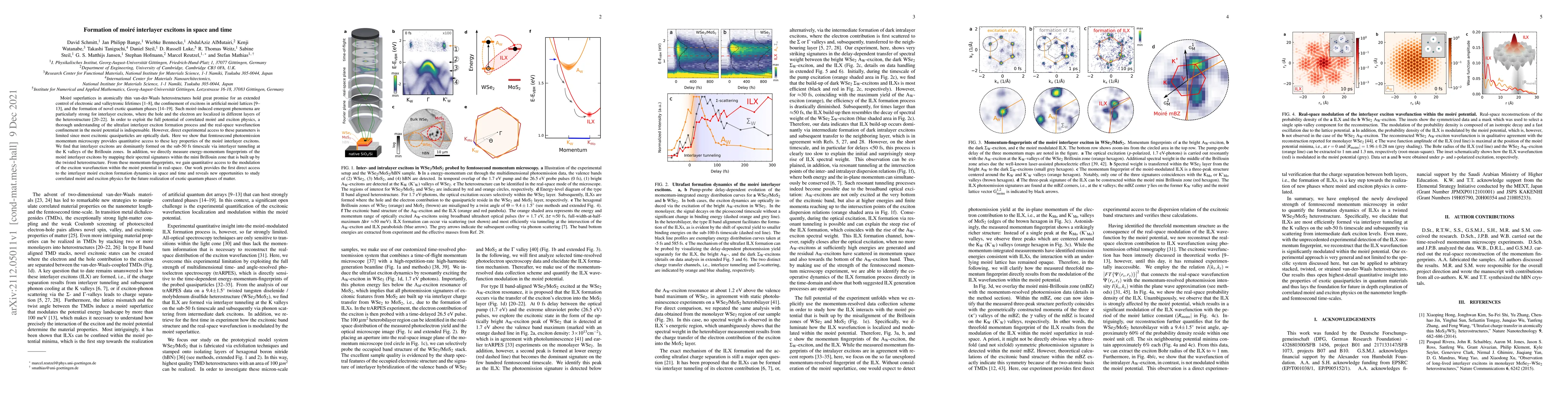
Moir\'e superlattices in atomically thin van-der-Waals heterostructures hold great promise for an extended control of electronic and valleytronic lifetimes, the confinement of excitons in artificial...
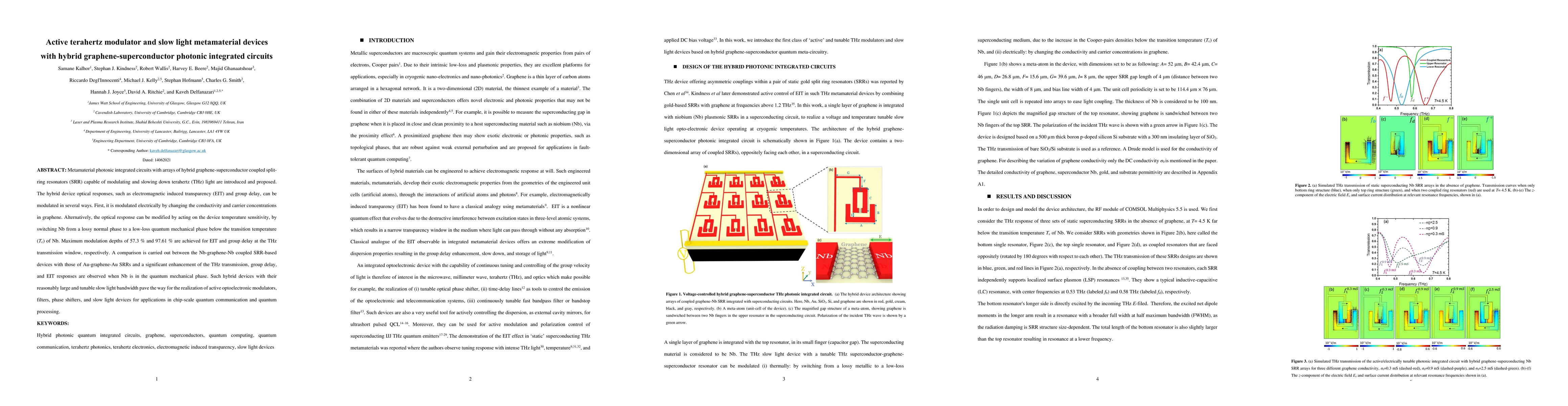
Metamaterial photonic integrated circuits with arrays of hybrid graphene-superconductor coupled split-ring resonators (SRR) capable of modulating and slowing down terahertz (THz) light are introduce...
Hexagonal boron nitride (h-BN) is well-established as a requisite support, encapsulant and barrier for 2D material technologies, but also recently as an active material for applications ranging from...
Structural defects are widely regarded as detrimental to the optoelectronic properties of monolayer transition metal dichalcogenides, leading to concerted efforts to eliminate defects via improved m...
The integration of two-dimensional (2D) materials with functional non-2D materials such as metal oxides is of key importance for many applications, but underlying mechanisms for such non-2D/2D inter...
Superconductivity can be induced in a normal material via the leakage of superconducting pairs of charge carriers from an adjacent superconductor. This so-called proximity effect is markedly influen...

2D materials research has reached significant scientific milestones, accompanied by a rapidly growing industrial sector in the two decades since the field's inception. Such rapid progress requires pus...
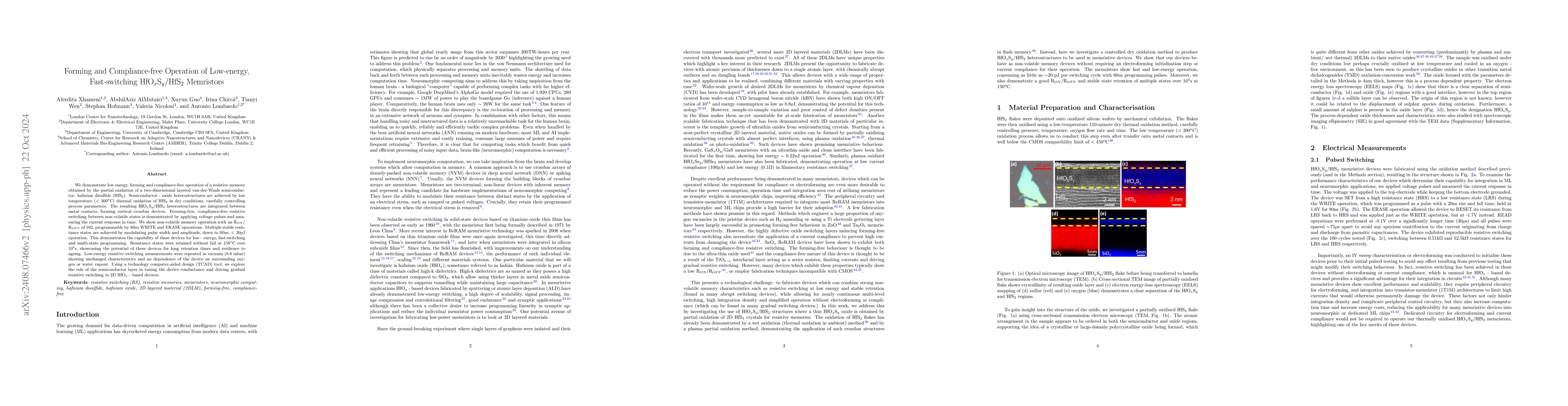
We demonstrate low energy, forming and compliance-free operation of a resistive memory obtained by the partial oxidation of a two-dimensional layered van-der-Waals semiconductor: hafnium disulfide (Hf...
Both tin monosulfide (SnS) and tin disulfide (SnS2) are thermodynamically stable layered materials with potential for spin-valleytronic devices and photodetectors. Notably, monolayer SnS, owing to its...
Over the past two decades, 2D materials have rapidly evolved into a diverse and expanding family of material platforms. Many members of this materials class have demonstrated their potential to delive...
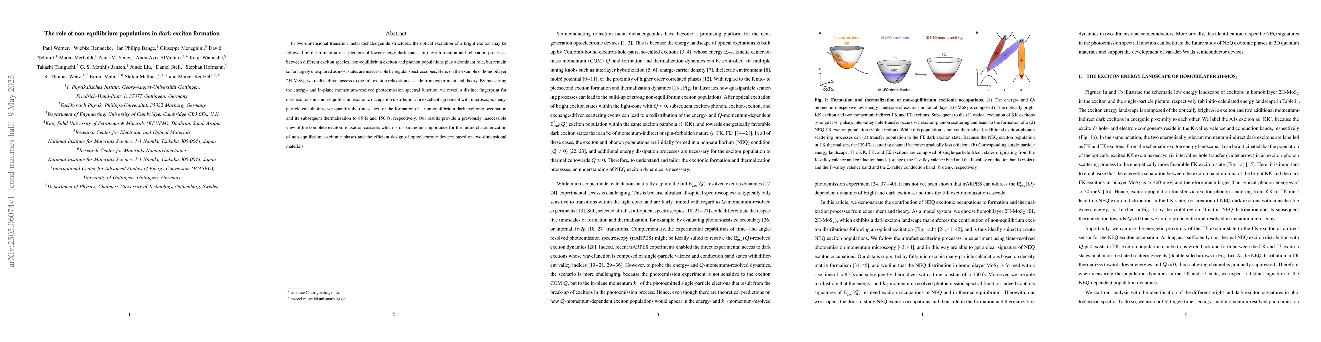
In two-dimensional transition metal dichalcogenide structures, the optical excitation of a bright exciton may be followed by the formation of a plethora of lower energy dark states. In these formation...