Publication
Metrics
AI Quick Summary
GFET Lab is an open-source, user-friendly software tool for simulating graphene field-effect transistors (GFETs), based on Jimenez's drain-current model with modifications for better predictive properties. The tool is validated against experimental data and can export SPICE-compatible models for circuit simulations.
Paper Preview
Abstract
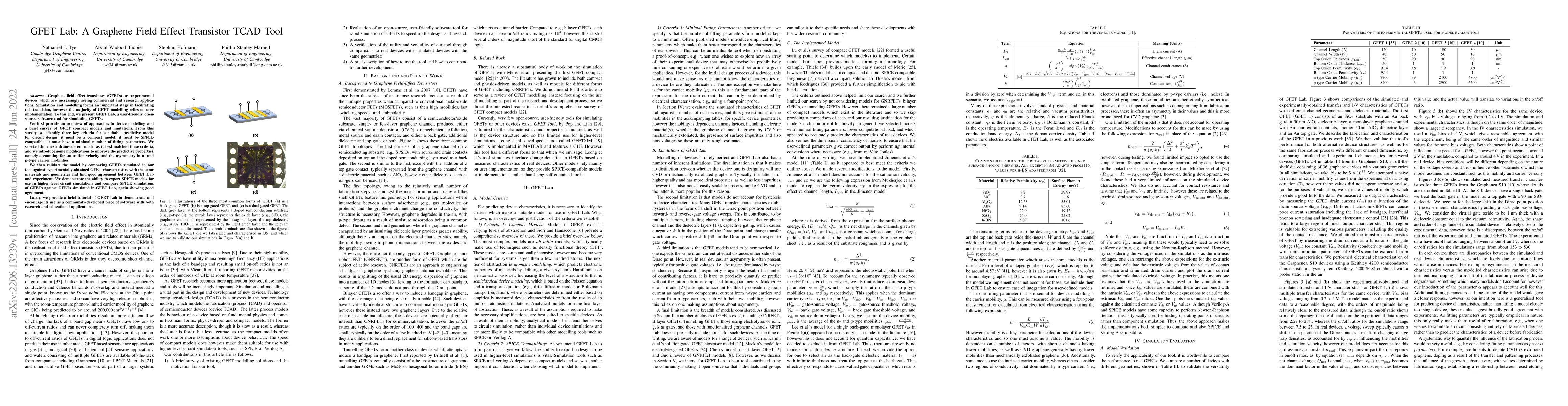
Graphene field-effect transistors (GFETs) are experimental devices which are increasingly seeing commercial and research applications. Simulation and modelling forms an important stage in facilitating this transition, however the majority of GFET modelling relies on user implementation. To this end, we present GFET Lab, a user-friendly, open-source software tool for simulating GFETs. We first provide an overview of approaches to device modelling and a brief survey of GFET compact models and limitations. From this survey, we identify three key criteria for a suitable predictive model for circuit design: it must be a compact model; it must be SPICE-compatible; it must have a minimal number of fitting parameters. We selected Jimenez's drain-current model as it best matched these criteria, and we introduce some modifications to improve the predictive properties, namely accounting for saturation velocity and the asymmetry in n- and p-type carrier mobilities. We then validate the model by comparing GFETs simulated in our tool against experimentally-obtained GFET characteristics with the same materials and geometries and find good agreement between GFET Lab and experiment. We demonstrate the ability to export SPICE models for use in higher level circuit simulations and compare SPICE simulations of GFETs against GFETs simulated in GFET Lab, again showing good agreement. Lastly, we provide a brief tutorial of GFET Lab to demonstrate and encourage its use as a community-developed piece of software with both research and educational applications.
AI Key Findings
Get AI-generated insights about this paper's methodology, results, significance, and more — seven facets brought into focus.
Impact
Paper Details
Authors
PDF Preview
Key Terms
Citation Network
Current paper (gray), citations (green), references (blue)
Display is limited for performance on very large graphs.
Discussion 0