Academic Profile
Statistics
Similar Authors
Papers on arXiv
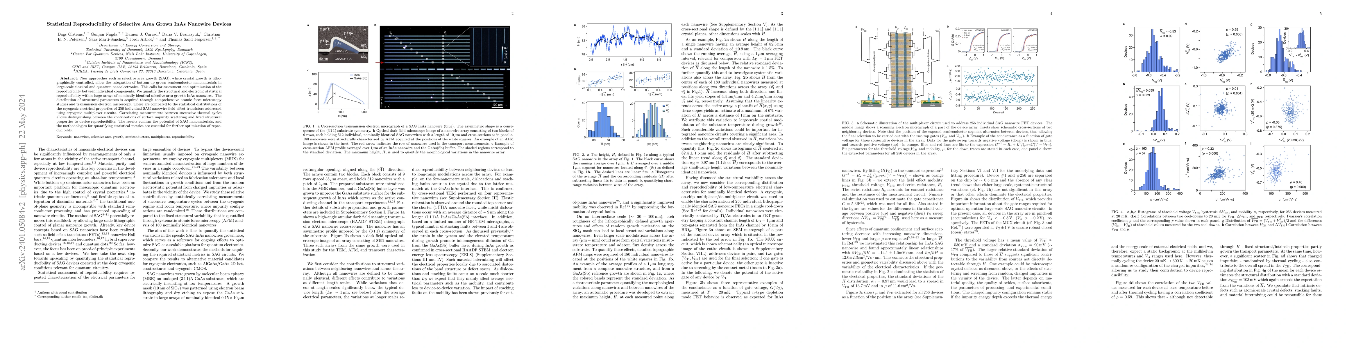
New approaches such as selective area growth, where crystal growth is lithographically controlled, allow the integration of bottom-up grown semiconductor nanomaterials in large-scale classical and q...
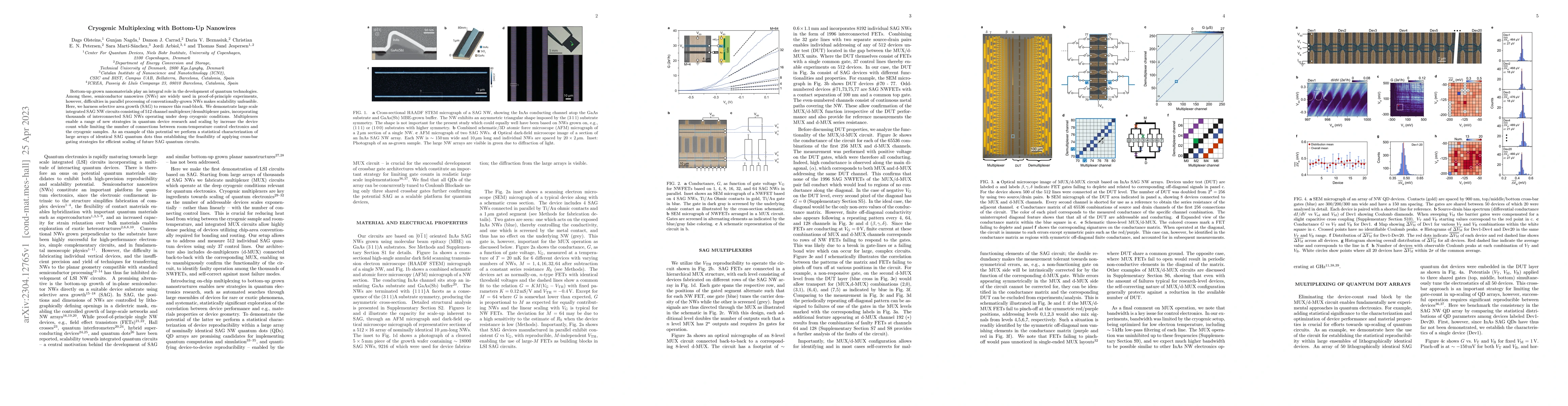
Bottom-up grown nanomaterials play an integral role in the development of quantum technologies. Among these, semiconductor nanowires (NWs) are widely used in proof-of-principle experiments, however,...
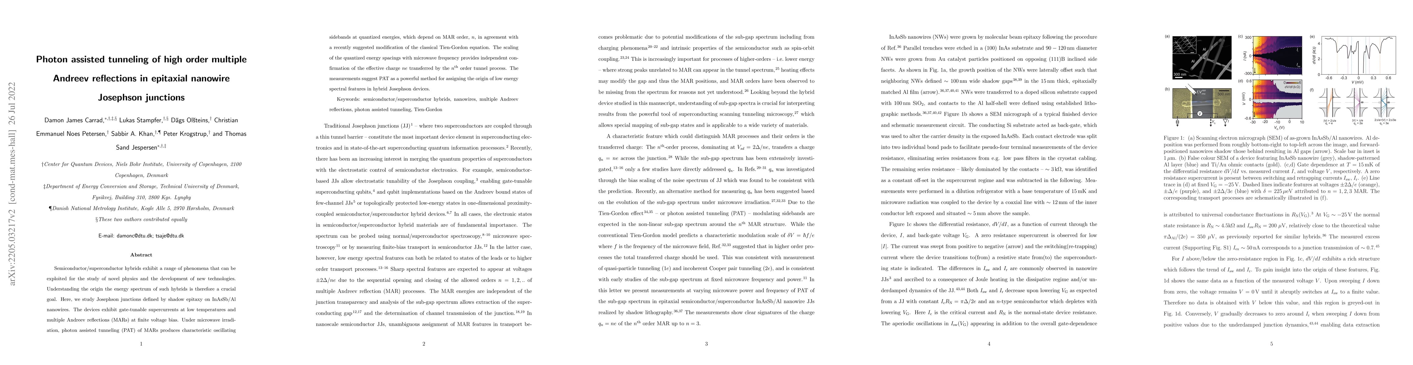
Semiconductor/superconductor hybrids exhibit a range of phenomena that can be exploited for the study of novel physics and the development of new technologies. Understanding the origin the energy sp...
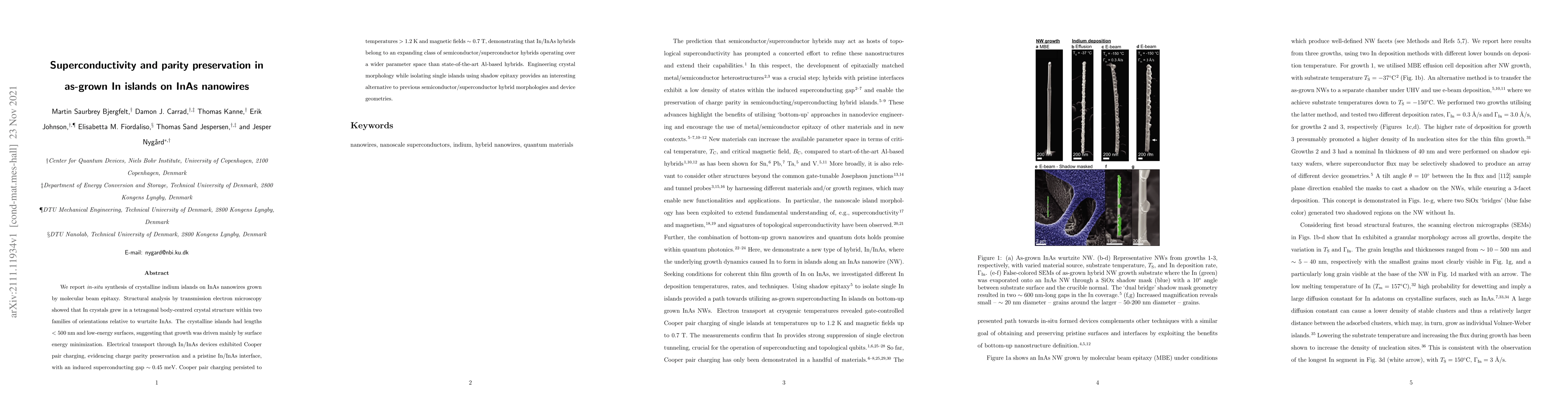
We report in-situ synthesis of crystalline indium islands on InAs nanowires grown by molecular beam epitaxy. Structural analysis by transmission electron microscopy showed that In crystals grew in a...
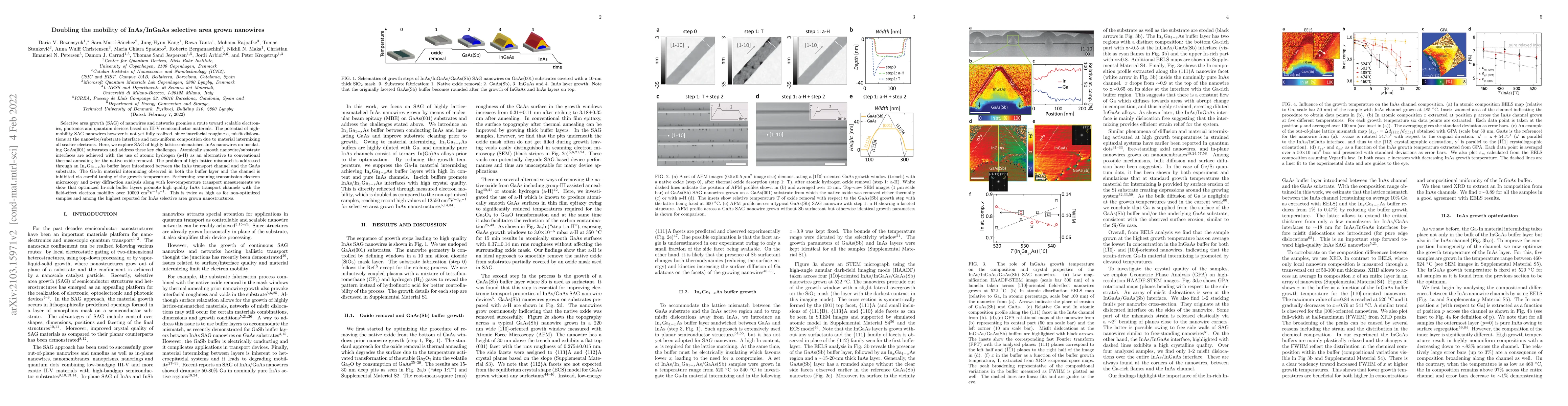
Selective area growth (SAG) of nanowires and networks promise a route toward scalable electronics, photonics and quantum devices based on III-V semiconductor materials. The potential of high-mobilit...
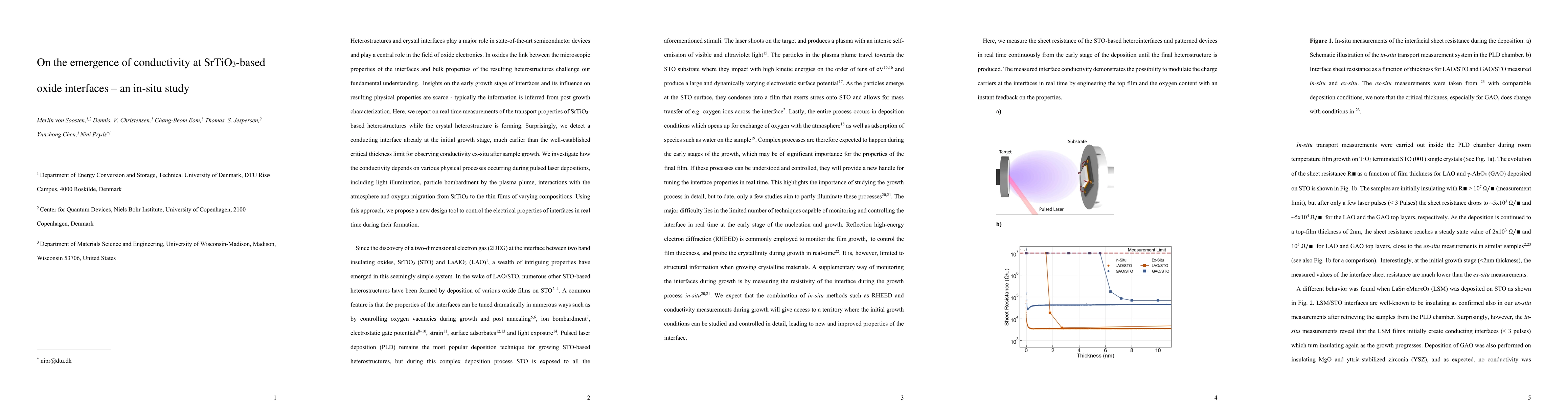
Heterostructures and crystal interfaces play a major role in state-of-the-art semiconductor devices and play a central role in the field of oxide electronics. In oxides the link between the microsco...
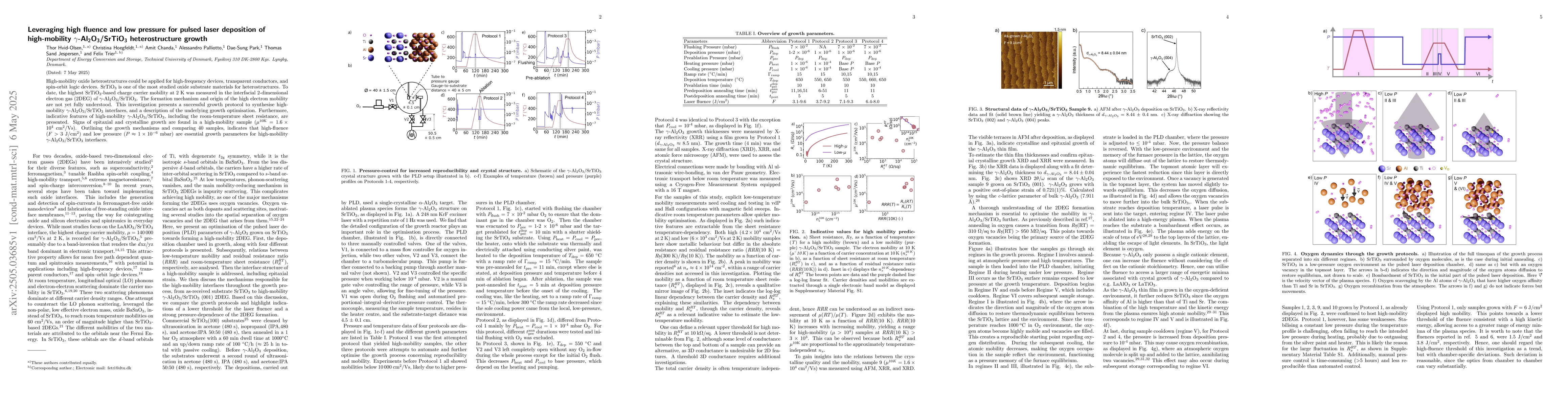
High-mobility oxide heterostructures could be applied for high-frequency devices, transparent conductors, and spin-orbit logic devices. SrTiO$_3$ is one of the most studied oxide substrate materials f...
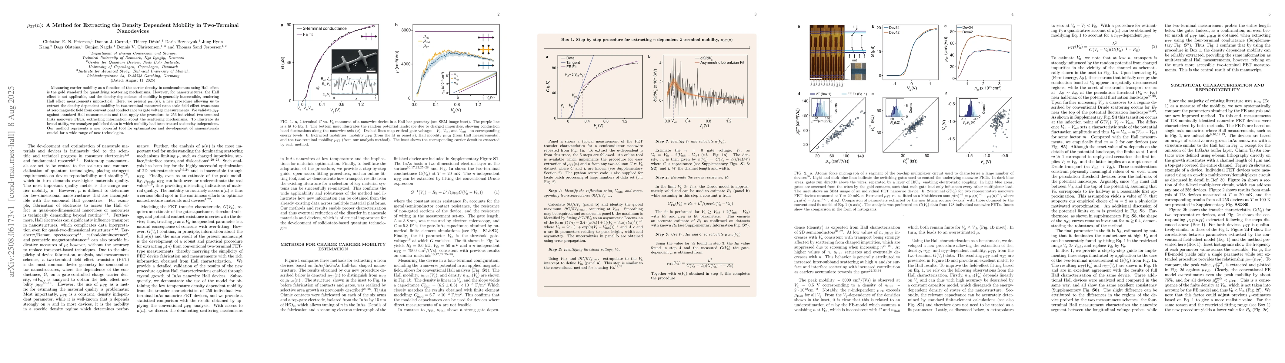
Measuring carrier mobility as a function of the carrier density in semiconductors using Hall effect is the gold standard for quantifying scattering mechanisms. However, for nanostructures, the Hall ef...
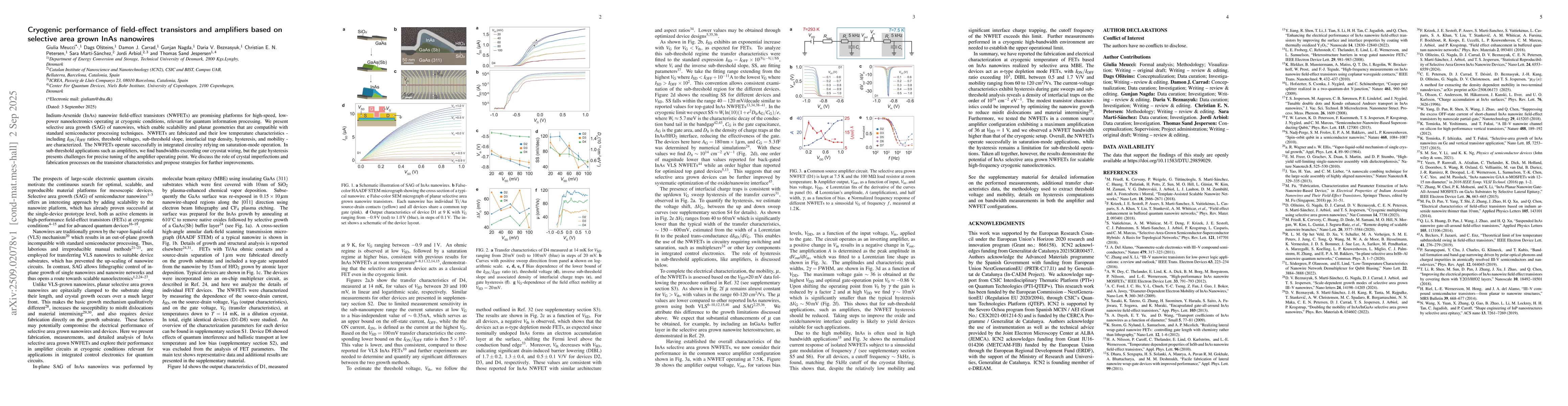
Indium-Arsenide (InAs) nanowire field-effect transistors (NWFETs) are promising platforms for high-speed, low power nanoelectronics operating at cryogenic conditions, relevant for quantum information ...
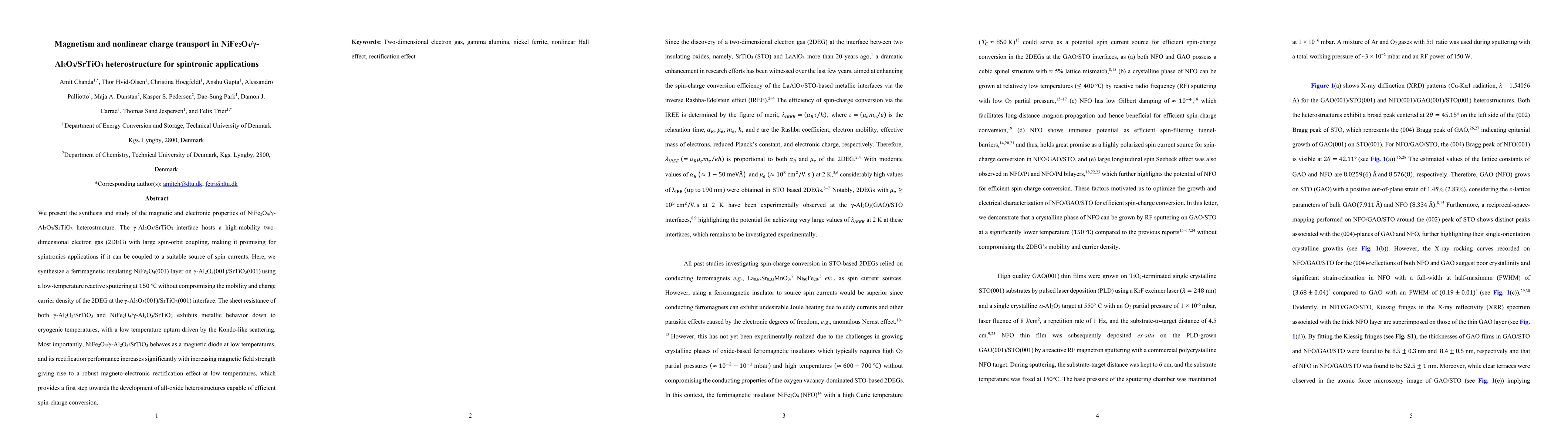
We present the synthesis and study of the magnetic and electronic properties of NiFe2O4/{\gamma}-Al2O3/SrTiO3 heterostructure. The {\gamma}-Al2O3/SrTiO3 interface hosts a high-mobility two-dimensional...
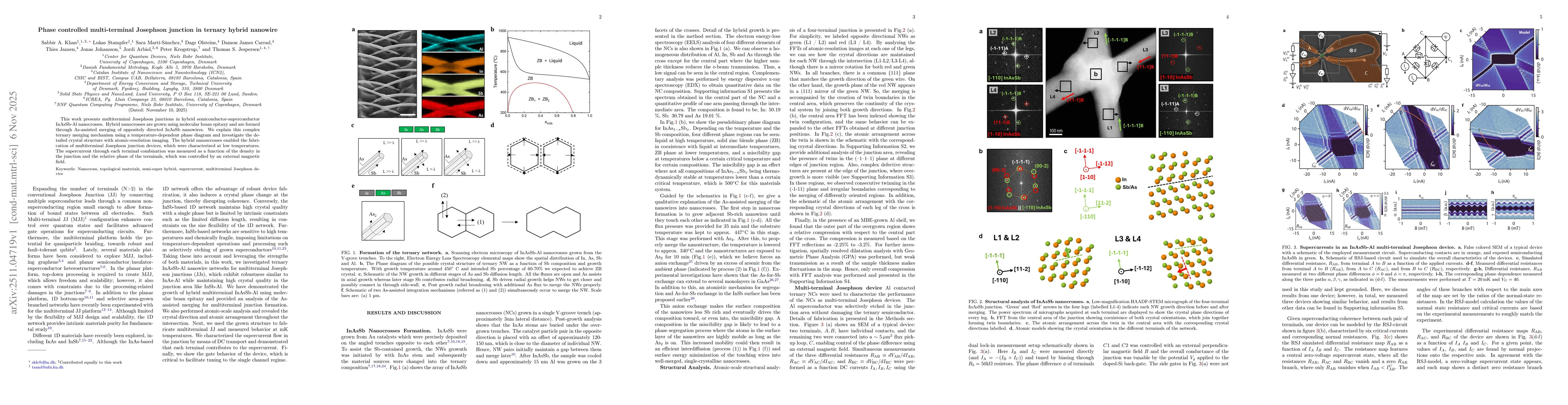
This work presents multiterminal Josephson junctions in hybrid semiconductor-superconductor InAsSb-Al nanocrosses. Hybrid nanocrosses are grown using molecular beam epitaxy and are formed through As-a...
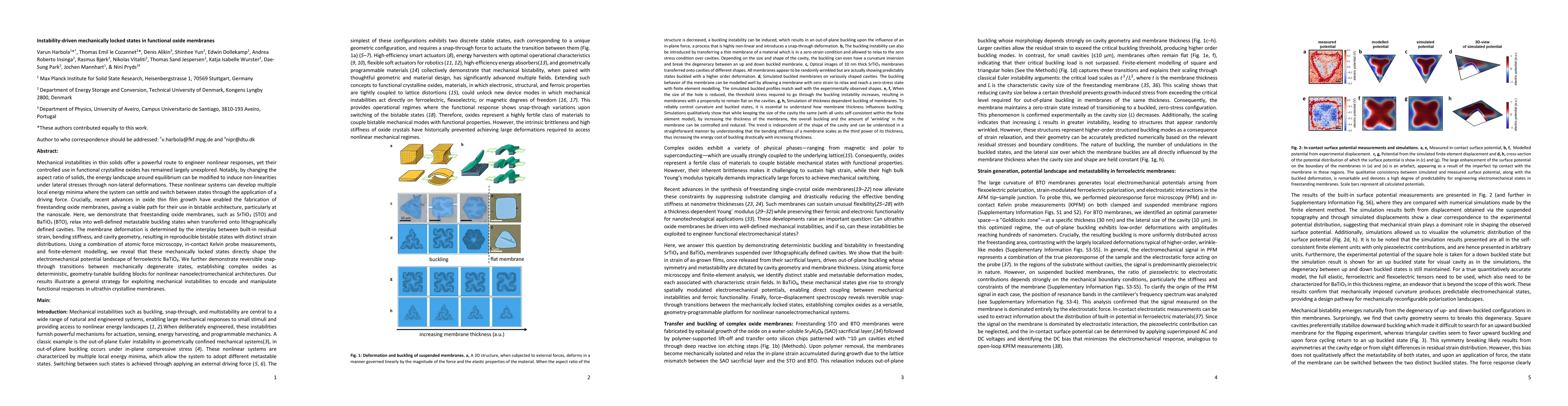
Mechanical instabilities in thin solids offer a powerful route to engineer nonlinear responses, yet their controlled use in functional crystalline oxides has remained largely unexplored. Notably, by c...
We study spin-resolved transport in a ballistic quantum dot with Rashba spin-orbit coupling, focusing on charge-to-spin conversion and spin Hall effect. In the regime where the dot size is comparable ...