Authors
Summary
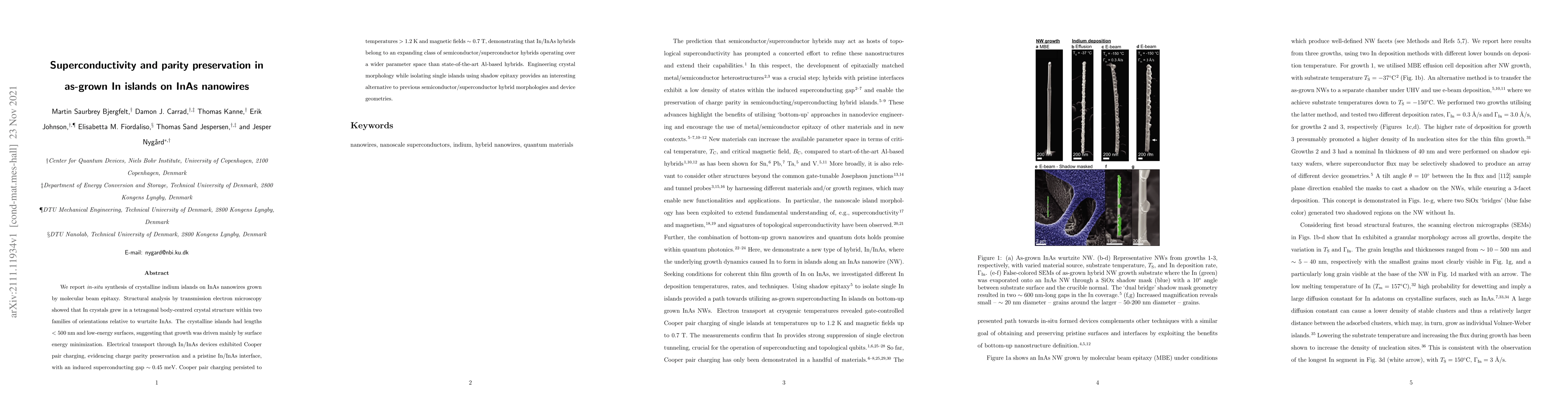
We report in-situ synthesis of crystalline indium islands on InAs nanowires grown by molecular beam epitaxy. Structural analysis by transmission electron microscopy showed that In crystals grew in a tetragonal body-centred crystal structure within two families of orientations relative to wurtzite InAs. The crystalline islands had lengths < 500 nm and low-energy surfaces, suggesting that growth was driven mainly by surface energy minimization. Electrical transport through In/InAs devices exhibited Cooper pair charging, evidencing charge parity preservation and a pristine In/InAs interface, with an induced superconducting gap ~ 0.45 meV. Cooper pair charging persisted to temperatures > 1.2 K and magnetic fields ~ 0.7 T, demonstrating that In/InAs hybrids belong to an expanding class of semiconductor/superconductor hybrids operating over a wider parameter space than state-of-the-art Al-based hybrids. Engineering crystal morphology while isolating single islands using shadow epitaxy provides an interesting alternative to previous semiconductor/superconductor hybrid morphologies and device geometries.
AI Key Findings
Get AI-generated insights about this paper's methodology, results, and significance.
Paper Details
PDF Preview
Key Terms
Citation Network
Current paper (gray), citations (green), references (blue)
Display is limited for performance on very large graphs.
Similar Papers
Found 4 papersCoulomb blockade in open superconducting islands on InAs nanowires
Jianhua Zhao, Hao Zhang, Yuqing Wang et al.
Sn/InAs Josephson junctions on selective area grown nanowires with in-situ shadowed superconductor evaporation
Hao Wu, Christopher J. Palmstrøm, Po Zhang et al.
Superconducting bistability in floating Al islands of hybrid Al/InAs nanowires
V. S. Khrapai, E. S. Tikhonov, E. V. Shpagina et al.
| Title | Authors | Year | Actions |
|---|
Comments (0)